JAJSFJ1 May   2018 DLPA4000

PRODUCTION DATA.  

  1. 特長
  2. アプリケーション
  3. 概要
    1.     Device Images
      1.      システム・ブロック図
  4. 改訂履歴
  5. 概要(続き)
  6. Pin Configuration and Functions
    1.     Pin Functions
  7. Specifications
    1. 7.1 Absolute Maximum Ratings
    2. 7.2 ESD Ratings
    3. 7.3 Recommended Operating Conditions
    4. 7.4 Thermal Information
    5. 7.5 Electrical Characteristics
    6. 7.6 SPI Timing Parameters
  8. Detailed Description
    1. 8.1 Overview
    2. 8.2 Functional Block Description
    3. 8.3 Feature Description
      1. 8.3.1 Supply and Monitoring
        1. 8.3.1.1 Supply
        2. 8.3.1.2 Monitoring
          1. 8.3.1.2.1 Block Faults
          2. 8.3.1.2.2 Low Battery and UVLO
          3. 8.3.1.2.3 Thermal Protection
      2. 8.3.2 Illumination
        1. 8.3.2.1 Programmable Gain Block
        2. 8.3.2.2 LDO Illumination
        3. 8.3.2.3 Illumination Driver A
        4. 8.3.2.4 External MOSFETs
          1. 8.3.2.4.1 Gate series resistor (RG)
          2. 8.3.2.4.2 Gate series diode (DG)
          3. 8.3.2.4.3 Gate parallel capacitance (CG)
        5. 8.3.2.5 RGB Strobe Decoder
          1. 8.3.2.5.1 Break Before Make (BBM)
          2. 8.3.2.5.2 Openloop Voltage
          3. 8.3.2.5.3 Transient Current Limit
        6. 8.3.2.6 Illumination Monitoring
          1. 8.3.2.6.1 Power Good
          2. 8.3.2.6.2 RatioMetric Overvoltage Protection
      3. 8.3.3 External Power MOSFET Selection
        1. 8.3.3.1 Threshold Voltage
        2. 8.3.3.2 Gate Charge and Gate Timing
        3. 8.3.3.3 On-resistance RDS(on)
      4. 8.3.4 DMD Supplies
        1. 8.3.4.1 LDO DMD
        2. 8.3.4.2 DMD HV Regulator
        3. 8.3.4.3 DMD/DLPC Buck Converters
        4. 8.3.4.4 DMD Monitoring
          1. 8.3.4.4.1 Power Good
          2. 8.3.4.4.2 Overvoltage Fault
      5. 8.3.5 Buck Converters
        1. 8.3.5.1 LDO Bucks
        2. 8.3.5.2 General Purpose Buck Converters
        3. 8.3.5.3 Buck Converter Monitoring
          1. 8.3.5.3.1 Power Good
          2. 8.3.5.3.2 Overvoltage Fault
      6. 8.3.6 Auxiliary LDOs
      7. 8.3.7 Measurement System
    4. 8.4 Device Functional Modes
    5. 8.5 Programming
      1. 8.5.1 SPI
      2. 8.5.2 Interrupt
      3. 8.5.3 Fast-Shutdown in Case of Fault
      4. 8.5.4 Protected Registers
      5. 8.5.5 Writing to EEPROM
    6. 8.6 Register Maps
  9. Application and Implementation
    1. 9.1 Application Information
    2. 9.2 Typical Application
      1. 9.2.1 Design Requirements
      2. 9.2.2 Detailed Design Procedure
        1. 9.2.2.1 Component Selection for General-Purpose Buck Converters
    3. 9.3 System Example With DLPA4000 Internal Block Diagram
  10. 10Power Supply Recommendations
    1. 10.1 Power-Up and Power-Down Timing
  11. 11Layout
    1. 11.1 Layout Guidelines
      1. 11.1.1 LED Driver
        1. 11.1.1.1 PowerBlock Gate Control Isolation
        2. 11.1.1.2 VIN to PowerBlocks
        3. 11.1.1.3 Return Current from LEDs and RSense
        4. 11.1.1.4 RC Snubber
        5. 11.1.1.5 Capacitor Choice
      2. 11.1.2 General Purpose Buck 2
      3. 11.1.3 SPI Connections
      4. 11.1.4 RLIM Routing
      5. 11.1.5 LED Connection
    2. 11.2 Layout Example
    3. 11.3 Thermal Considerations
  12. 12デバイスおよびドキュメントのサポート
    1. 12.1 デバイス・サポート
      1. 12.1.1 デバイスの項目表記
    2. 12.2 ドキュメントの更新通知を受け取る方法
    3. 12.3 コミュニティ・リソース
    4. 12.4 商標
    5. 12.5 静電気放電に関する注意事項
    6. 12.6 Glossary
  13. 13メカニカル、パッケージ、および注文情報
    1. 13.1 Package Option Addendum
      1. 13.1.1 Packaging Information

パッケージ・オプション

メカニカル・データ(パッケージ|ピン)
サーマルパッド・メカニカル・データ
発注情報

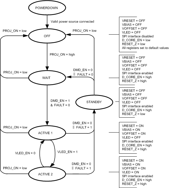
Device Functional Modes

Table 4. Modes of Operation

MODE DESCRIPTION
OFF This is the lowest-power mode of operation. All power functions are de-energized, registers are reset to their default values, and the IC does not respond to SPI commands. RESET_Z pin is pulled low. The IC enters OFF mode whenever the PROJ_ON pin is low.
WAIT The DMD regulators and LED power (VLED) are turned off, but the IC does respond to the SPI. The device enters WAIT mode whenever PROJ_ON is set high, DMD_EN(1) bit is set to 0 or a FAULT is resolved.
STANDBY The device also enters STANDBY mode when a fault condition is detected(2). (See also section Interrupt). Once the fault condition is resolved, WAIT mode is entered.
ACTIVE1 The DMD supplies are enabled but LED power (VLED) is disabled. PROJ_ON pin must be high, DMD_EN bit must be set to 1, and ILLUM_EN(3) bit is set to 0.
ACTIVE2 DMD supplies and LED power are enabled. PROJ_ON pin must be high and DMD_EN and ILLUM_EN bits must both be set to 1.
Settings can be done through register 0x01
Power-good faults, over-voltage, over-temperature shutdown, and undervoltage lockout
Settings can be done through register 0x01, bit is named ILLUM_EN

Table 5. Device State as a Function of Control-Pin Status

PROJ_ON Pin STATE
LOW OFF
HIGH WAIT
STANDBY
ACTIVE1
ACTIVE2
(Device state depends on DMD_EN and ILLUM_EN bits and whether there are any fault conditions.)
DLPA4000 State_Diagram.gif
|| = OR, & = AND
FAULT = Undervoltage on any supply, thermal shutdown, or UVLO detection
UVLO detection, per the diagram, causes the DLPA4000 to go into the standby state. Standby state is not the lowest power state. If the application requires lower power, set PROJ_ON low.
DMD_EN register bit can be reset or set by SPI writes. DMD_EN defaults to 0 when PROJ_ON goes from low to high and then the DLPC4422 software automatically sets it to 1. Also, FAULT = 1 causes the DMD_EN register bit to be reset.
D_CORE_EN is a signal internal to the DLPA4000. This signal turns on the VCORE regulator.
Figure 18. State Diagram