JAJSFJ1 May   2018 DLPA4000

PRODUCTION DATA.  

  1. 特長
  2. アプリケーション
  3. 概要
    1.     Device Images
      1.      システム・ブロック図
  4. 改訂履歴
  5. 概要(続き)
  6. Pin Configuration and Functions
    1.     Pin Functions
  7. Specifications
    1. 7.1 Absolute Maximum Ratings
    2. 7.2 ESD Ratings
    3. 7.3 Recommended Operating Conditions
    4. 7.4 Thermal Information
    5. 7.5 Electrical Characteristics
    6. 7.6 SPI Timing Parameters
  8. Detailed Description
    1. 8.1 Overview
    2. 8.2 Functional Block Description
    3. 8.3 Feature Description
      1. 8.3.1 Supply and Monitoring
        1. 8.3.1.1 Supply
        2. 8.3.1.2 Monitoring
          1. 8.3.1.2.1 Block Faults
          2. 8.3.1.2.2 Low Battery and UVLO
          3. 8.3.1.2.3 Thermal Protection
      2. 8.3.2 Illumination
        1. 8.3.2.1 Programmable Gain Block
        2. 8.3.2.2 LDO Illumination
        3. 8.3.2.3 Illumination Driver A
        4. 8.3.2.4 External MOSFETs
          1. 8.3.2.4.1 Gate series resistor (RG)
          2. 8.3.2.4.2 Gate series diode (DG)
          3. 8.3.2.4.3 Gate parallel capacitance (CG)
        5. 8.3.2.5 RGB Strobe Decoder
          1. 8.3.2.5.1 Break Before Make (BBM)
          2. 8.3.2.5.2 Openloop Voltage
          3. 8.3.2.5.3 Transient Current Limit
        6. 8.3.2.6 Illumination Monitoring
          1. 8.3.2.6.1 Power Good
          2. 8.3.2.6.2 RatioMetric Overvoltage Protection
      3. 8.3.3 External Power MOSFET Selection
        1. 8.3.3.1 Threshold Voltage
        2. 8.3.3.2 Gate Charge and Gate Timing
        3. 8.3.3.3 On-resistance RDS(on)
      4. 8.3.4 DMD Supplies
        1. 8.3.4.1 LDO DMD
        2. 8.3.4.2 DMD HV Regulator
        3. 8.3.4.3 DMD/DLPC Buck Converters
        4. 8.3.4.4 DMD Monitoring
          1. 8.3.4.4.1 Power Good
          2. 8.3.4.4.2 Overvoltage Fault
      5. 8.3.5 Buck Converters
        1. 8.3.5.1 LDO Bucks
        2. 8.3.5.2 General Purpose Buck Converters
        3. 8.3.5.3 Buck Converter Monitoring
          1. 8.3.5.3.1 Power Good
          2. 8.3.5.3.2 Overvoltage Fault
      6. 8.3.6 Auxiliary LDOs
      7. 8.3.7 Measurement System
    4. 8.4 Device Functional Modes
    5. 8.5 Programming
      1. 8.5.1 SPI
      2. 8.5.2 Interrupt
      3. 8.5.3 Fast-Shutdown in Case of Fault
      4. 8.5.4 Protected Registers
      5. 8.5.5 Writing to EEPROM
    6. 8.6 Register Maps
  9. Application and Implementation
    1. 9.1 Application Information
    2. 9.2 Typical Application
      1. 9.2.1 Design Requirements
      2. 9.2.2 Detailed Design Procedure
        1. 9.2.2.1 Component Selection for General-Purpose Buck Converters
    3. 9.3 System Example With DLPA4000 Internal Block Diagram
  10. 10Power Supply Recommendations
    1. 10.1 Power-Up and Power-Down Timing
  11. 11Layout
    1. 11.1 Layout Guidelines
      1. 11.1.1 LED Driver
        1. 11.1.1.1 PowerBlock Gate Control Isolation
        2. 11.1.1.2 VIN to PowerBlocks
        3. 11.1.1.3 Return Current from LEDs and RSense
        4. 11.1.1.4 RC Snubber
        5. 11.1.1.5 Capacitor Choice
      2. 11.1.2 General Purpose Buck 2
      3. 11.1.3 SPI Connections
      4. 11.1.4 RLIM Routing
      5. 11.1.5 LED Connection
    2. 11.2 Layout Example
    3. 11.3 Thermal Considerations
  12. 12デバイスおよびドキュメントのサポート
    1. 12.1 デバイス・サポート
      1. 12.1.1 デバイスの項目表記
    2. 12.2 ドキュメントの更新通知を受け取る方法
    3. 12.3 コミュニティ・リソース
    4. 12.4 商標
    5. 12.5 静電気放電に関する注意事項
    6. 12.6 Glossary
  13. 13メカニカル、パッケージ、および注文情報
    1. 13.1 Package Option Addendum
      1. 13.1.1 Packaging Information

パッケージ・オプション

メカニカル・データ(パッケージ|ピン)
サーマルパッド・メカニカル・データ
発注情報

SPI

The DLPA4000 provides a 4-wire SPI port that supports two SPI clock frequency modes: 0 MHz to 36 MHz and 20 MHz to 40MHz. The clock frequency mode can be set in register 0x17, DIG_SPI_FAST_SEL. The interface supports both read and write operations. The SPI_SS_Z input serves as the active low chip select for the SPI port. The SPI_SS_Z input must be forced low for writing to or reading from registers. When SPI_SS_Z is forced high, the data at the SPI_MOSI input is ignored, and the SPI_MISO output is forced to a high-impedance state. The SPI_MOSI input serves as the serial data input for the port; the SPI_MISO output serves as the serial data output. The SPI_CLK input serves as the serial data clock for both the input and output data. Data at the SPI_MOSI input is latched on the rising edge of SPI_CLK, while data is clocked out of the SPI_MISO output on the falling edge of SPI_CLK. Figure 19 illustrates the SPI port protocol. Byte 0 is referred to as the command byte, where the most significant bit is the write/not-read bit. For the W/nR bit, a 1 indicates a write operation, while a 0 indicates a read operation. The remaining seven bits of the command byte are the register address targeted by the write or read operation. The SPI port supports write and read operations for multiple sequential register addresses through the implementation of an auto-increment mode. As shown in Figure 19, the auto-increment mode is invoked by simply holding the SPI_SS_Z input low for multiple data bytes. The register address is automatically incremented after each data byte transferred, starting with the address specified by the command byte. After reaching address 0x7Fh the address pointer jumps back to 0x00h.
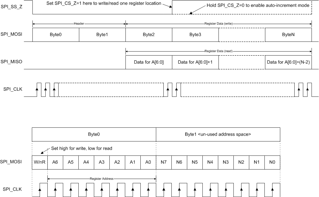
DLPA4000 SPI_Protocol.gifFigure 19. SPI Protocol
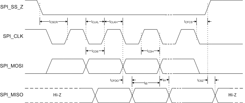
DLPA4000 SPI_Timing.gifFigure 20. SPI Timing Diagram