JAJSHN0F July 2014 – November 2020 DLPC3430 , DLPC3435
PRODUCTION DATA
- 1 特長
- 2 アプリケーション
- 3 概要
- 4 Revision History
- 5 Pin Configuration and Functions
-
6 Specifications
- 6.1 Absolute Maximum Ratings
- 6.2 ESD Ratings
- 6.3 Recommended Operating Conditions
- 6.4 Thermal Information
- 6.5 Power Electrical Characteristics
- 6.6 Pin Electrical Characteristics
- 6.7 Internal Pullup and Pulldown Electrical Characteristics
- 6.8 DMD Sub-LVDS Interface Electrical Characteristics
- 6.9 DMD Low-Speed Interface Electrical Characteristics
- 6.10 System Oscillator Timing Requirements
- 6.11 Power Supply and Reset Timing Requirements
- 6.12 Parallel Interface Frame Timing Requirements
- 6.13 Parallel Interface General Timing Requirements
- 6.14 BT656 Interface General Timing Requirements
- 6.15 DSI Host Timing Requirements
- 6.16 Flash Interface Timing Requirements
- 6.17 Other Timing Requirements
- 6.18 DMD Sub-LVDS Interface Switching Characteristics
- 6.19 DMD Parking Switching Characteristics
- 6.20 Chipset Component Usage Specification
-
7 Detailed Description
- 7.1 Overview
- 7.2 Functional Block Diagram
- 7.3 Feature Description
- 7.4 Device Functional Modes
- 7.5 Programming
- 8 Application and Implementation
- 9 Power Supply Recommendations
- 10Layout
- 11Device and Documentation Support
- 12Mechanical, Packaging, and Orderable Information
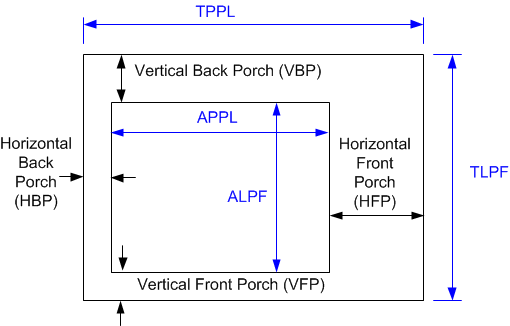
11.1.2.2 Video Timing Parameter Definitions
See Figure 11-1 for a visual description.
- Active Lines Per Frame (ALPF)Defines the number of lines in a frame containing displayable data. ALPF is a subset of the TLPF.
- Active Pixels Per Line (APPL)Defines the number of pixel clocks in a line containing displayable data. APPL is a subset of the TPPL.
- Horizontal Back Porch (HBP) BlankingDefines the number of blank pixel clocks after the active edge of horizontal sync but before the first active pixel.
- Horizontal Front Porch (HFP) BlankingDefines the number of blank pixel clocks after the last active pixel but before horizontal sync.
- Horizontal Sync (HS or Hsync)Timing reference point that defines the start of each horizontal interval (line). The active edge of the HS signal defines the absolute reference point. The active edge (either rising or falling edge as defined by the source) is the reference from which all horizontal blanking parameters are measured.
- Total Lines Per Frame (TLPF)Total number of active and inactive lines per frame; defines the vertical period (or frame time).
- Total Pixel Per Line (TPPL)Total number of active and inactive pixel clocks per line; defines the horizontal line period in pixel clocks.
- Vertical Sync (VS or Vsync)Timing reference point that defines the start of the vertical interval (frame). The absolute reference point is defined by the active edge of the VS signal. The active edge (either rising or falling edge as defined by the source) is the reference from which all vertical blanking parameters are measured.
- Vertical Back Porch (VBP) BlankingDefines the number of blank lines after the active edge of vertical sync but before the first active line.
- Vertical Front Porch (VFP) BlankingDefines the number of blank lines after the last active line but before the active edge of vertical sync.
 Figure 11-1 Parameter Definitions