JAJSFC5C April   2018  – December 2020 DLPC3470

PRODUCTION DATA  

  1. 特長
  2. アプリケーション
  3. 概要
  4. Revision History
  5. Pin Configuration and Functions
  6. Specifications
    1. 6.1  Absolute Maximum Ratings
    2. 6.2  ESD Ratings
    3. 6.3  Recommended Operating Conditions
    4. 6.4  Thermal Information
    5. 6.5  Power Electrical Characteristics
    6. 6.6  Pin Electrical Characteristics
    7. 6.7  Internal Pullup and Pulldown Electrical Characteristics
    8. 6.8  DMD Sub-LVDS Interface Electrical Characteristics
    9. 6.9  DMD Low-Speed Interface Electrical Characteristics
    10. 6.10 System Oscillator Timing Requirements
    11. 6.11 Power Supply and Reset Timing Requirements
    12. 6.12 Parallel Interface Frame Timing Requirements
    13. 6.13 Parallel Interface General Timing Requirements
    14. 6.14 BT656 Interface General Timing Requirements
    15. 6.15 Flash Interface Timing Requirements
    16. 6.16 Other Timing Requirements
    17. 6.17 DMD Sub-LVDS Interface Switching Characteristics
    18. 6.18 DMD Parking Switching Characteristics
    19. 6.19 Chipset Component Usage Specification
  7. Detailed Description
    1. 7.1 Overview
    2. 7.2 Functional Block Diagram
    3. 7.3 Feature Description
      1. 7.3.1  Input Source
        1. 7.3.1.1 Supported Resolution and Frame Rates
        2. 7.3.1.2 3-D Display
        3. 7.3.1.3 Parallel Interface
          1. 7.3.1.3.1 PDATA Bus – Parallel Interface Bit Mapping Modes
      2. 7.3.2  Pattern Display
        1. 7.3.2.1 External Pattern Mode
          1. 7.3.2.1.1 8-bit Monochrome Patterns
          2. 7.3.2.1.2 1-Bit Monochrome Patterns
        2. 7.3.2.2 Internal Pattern Mode
          1. 7.3.2.2.1 Free Running Mode
          2. 7.3.2.2.2 Trigger In Mode
      3. 7.3.3  Device Startup
      4. 7.3.4  SPI Flash
        1. 7.3.4.1 SPI Flash Interface
        2. 7.3.4.2 SPI Flash Programming
      5. 7.3.5  I2C Interface
      6. 7.3.6  Content Adaptive Illumination Control (CAIC)
      7. 7.3.7  Local Area Brightness Boost (LABB)
      8. 7.3.8  3D Glasses Operation
      9. 7.3.9  Test Point Support
      10. 7.3.10 DMD Interface
        1. 7.3.10.1 Sub-LVDS (HS) Interface
    4. 7.4 Device Functional Modes
    5. 7.5 Programming
  8. Application and Implementation
    1. 8.1 Application Information
    2. 8.2 Typical Application
      1. 8.2.1 Pattern projector for 3D depth scanning
        1. 8.2.1.1 Design Requirements
        2. 8.2.1.2 Detailed Design Procedure
        3. 8.2.1.3 Application Curve
      2. 8.2.2 Pattern Projector with Internal Streaming Mode
        1. 8.2.2.1 Design Requirements
        2. 8.2.2.2 Detailed Design Procedure
        3. 8.2.2.3 Application Curve
  9. Power Supply Recommendations
    1. 9.1 PLL Design Considerations
    2. 9.2 System Power-Up and Power-Down Sequence
    3. 9.3 Power-Up Initialization Sequence
    4. 9.4 DMD Fast Park Control (PARKZ)
    5. 9.5 Hot Plug I/O Usage
  10. 10Layout
    1. 10.1 Layout Guidelines
      1. 10.1.1 PLL Power Layout
      2. 10.1.2 Reference Clock Layout
        1. 10.1.2.1 Recommended Crystal Oscillator Configuration
      3. 10.1.3 Unused Pins
      4. 10.1.4 DMD Control and Sub-LVDS Signals
      5. 10.1.5 Layer Changes
      6. 10.1.6 Stubs
      7. 10.1.7 Terminations
      8. 10.1.8 Routing Vias
      9. 10.1.9 Thermal Considerations
    2. 10.2 Layout Example
  11. 11Device and Documentation Support
    1. 11.1 Device Support
      1. 11.1.1 Third-Party Products Disclaimer
      2. 11.1.2 Device Nomenclature
        1. 11.1.2.1 Device Markings
      3. 11.1.3 Video Timing Parameter Definitions
    2. 11.2 Related Documentation
    3. 11.3 ドキュメントの更新通知を受け取る方法
    4. 11.4 サポート・リソース
    5. 11.5 Trademarks
    6. 11.6 静電気放電に関する注意事項
    7. 11.7 用語集
  12. 12Mechanical, Packaging, and Orderable Information

パッケージ・オプション

メカニカル・データ(パッケージ|ピン)
サーマルパッド・メカニカル・データ
発注情報

Internal Pattern Mode

There are two key differences between internal and external pattern mode:

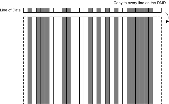
  • Internal pattern mode only supports 1D patterns i.e the pattern data is the same across the entire row or column of the DMD (Figure 7-12, Figure 7-13).
  • Internal pattern mode enables user to design a simple system by eliminating need of an external processor to generate and send patterns every frame. In internal pattern mode one row or one column patterns are pre-loaded in the flash memory and a command is send to DLPC3470 controller to display the patterns. Implementation details on how to create patterns, save patterns in Flash memory and load patterns from flash memory into the DLPC3470 controller’s internal memory are described in Software Programmers Guide.
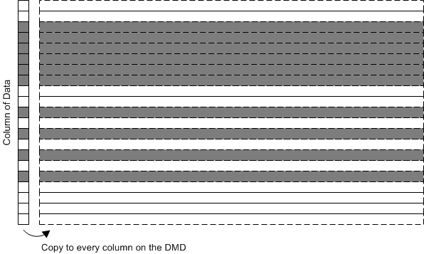
GUID-04BF98FE-C8C6-40B6-98AB-E552A058434E-low.gif Figure 7-12 Column Replication
GUID-FF4DBB34-27C1-4DBD-8C0B-575972B4A344-low.gif Figure 7-13 Row Replication

Internal pattern mode additionally provides two configurations to trigger the display of patterns, free running mode (shown in Figure 7-14) and trigger in mode (shown in Figure 7-15).