DLPS253 September 2024 DLPC8445
PRODUCTION DATA
- 1
- 1 Features
- 2 Applications
- 3 Description
-
4 Pin Configuration and Functions
- 6
- 4.1 Initialization, Board Level Test, and Debug
- 4.2 V-by-One Interface Input Data and Control
- 4.3 FPD Link Port(s) Input Data and Control (Not Supported in DLPC8445)
- 4.4 DSI Input Data and Clock (Not Supported in DLPC8445)
- 4.5 DMD SubLVDS Interface
- 4.6 DMD Reset and Low Speed Interfaces
- 4.7 Flash Interface
- 4.8 Peripheral Interfaces
- 4.9 GPIO Peripheral Interface
- 4.10 Clock and PLL Support
- 4.11 Power and Ground
- 4.12 I/O Type Subscript Definition
- 4.13 Internal Pullup and Pulldown Characteristics
-
5 Specifications
- 5.1 Absolute Maximum Ratings
- 22
- 5.2 ESD Ratings
- 5.3 Recommended Operating Conditions
- 5.4 Thermal Information
- 5.5 Power Electrical Characteristics
- 5.6 Pin Electrical Characteristics
- 5.7 DMD SubLVDS Interface Electrical Characteristics
- 29
- 5.8 DMD Low Speed Interface Electrical Characteristics
- 31
- 5.9 V-by-One Interface Electrical Characteristics
- 5.10 USB Electrical Characteristics
- 34
- 5.11 System Oscillator Timing Requirements
- 36
- 5.12 Power Supply and Reset Timing Requirements
- 38
- 5.13 V-by-One Interface General Timing Requirements
- 40
- 5.14 Flash Interface Timing Requirements
- 42
- 5.15 Source Frame Timing Requirements
- 44
- 5.16 Synchronous Serial Port Interface Timing Requirements
- 46
- 5.17 I2C Interface Timing Requirements
- 5.18 Programmable Output Clock Timing Requirements
- 5.19 JTAG Boundary Scan Interface Timing Requirements (Debug Only)
- 50
- 5.20 DMD Low Speed Interface Timing Requirements
- 52
- 5.21 DMD SubLVDS Interface Timing Requirements
- 6 Detailed Description
- 7 Power Supply Recommendations
- 8 Layout
- 9 Device and Documentation Support
- 10Revision History
- 11Mechanical, Packaging, and Orderable Information
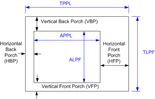
9.8.1 Video Timing Parameter Definitions
- Active Lines Per Frame (ALPF)Defines the number of lines in a frame containing displayable data: ALPF is a subset of the TLPF.
- Active Pixels Per Line (APPL)Defines the number of pixel clocks in a line containing displayable data: APPL is a subset of the TPPL.
- Horizontal Back Porch (HBP) BlankingNumber of blank pixel clocks after horizontal sync but before the first active pixel. Note: HBP times are reference to the leading (active) edge of the respective sync signal.
- Horizontal Front Porch (HFP) BlankingNumber of blank pixel clocks after the last active pixel but before Horizontal Sync.
- Horizontal Sync (HS)Timing reference point that defines the start of each horizontal interval (line). The absolute reference point is defined by the active edge of the HS signal. The active edge (either rising or falling edge as defined by the source) is the reference from which all horizontal blanking parameters are measured.
- Total Lines Per Frame (TLPF)Defines the vertical period (or frame time) in lines: TLPF = Total number of lines per frame (active and inactive).
- Total Pixel Per Line (TPPL)Defines the horizontal line period in pixel clocks: TPPL = Total number of pixel clocks per line (active and inactive).
- Vertical Sync (VS)Timing reference point that defines the start of the vertical interval (frame). The absolute reference point is defined by the active edge of the VS signal. The active edge (either rising or falling edge as defined by the source) is the reference from which all vertical blanking parameters are measured.
- Vertical Back Porch (VBP) BlankingNumber of blank lines after vertical sync but before the first active line.
- Vertical Front Porch (VFP) BlankingNumber of blank lines after the last active line but before vertical sync.