JAJSLL2B April 2021 – November 2021 DP83561-SP
PRODUCTION DATA
- 1 特長
- 2 アプリケーション
- 3 概要
- 4 Revision History
- 5 Pin Configuration and Functions
- 6 Specifications
-
7 Detailed Description
- 7.1 Overview
- 7.2 Functional Block Diagram
- 7.3
Feature Description
- 7.3.1 Copper Ethernet
- 7.3.2 MAC Interfaces
- 7.3.3
Auto-Negotiation
- 7.3.3.1 Speed and Duplex Selection - Priority Resolution
- 7.3.3.2 Master and Slave Resolution
- 7.3.3.3 Pause and Asymmetrical Pause Resolution
- 7.3.3.4 Next Page Support
- 7.3.3.5 Parallel Detection
- 7.3.3.6 Restart Auto-Negotiation
- 7.3.3.7 Enabling Auto-Negotiation Through Software
- 7.3.3.8 Auto-Negotiation Complete Time
- 7.3.3.9 Auto-MDIX Resolution
- 7.3.4 Speed Optimization
- 7.3.5 Radiation Performance
- 7.3.6 WoL (Wake-on-LAN) Packet Detection
- 7.3.7 Start of Frame Detect for IEEE 1588 Time Stamp
- 7.3.8 Cable Diagnostics
- 7.3.9 Clock Output
- 7.4 Device Functional Modes
- 7.5
Programming
- 7.5.1
Serial Management Interface
- 7.5.1.1
Extended Address Space Access
- 7.5.1.1.1 Write Address Operation
- 7.5.1.1.2 Read Address Operation
- 7.5.1.1.3 Write (No Post Increment) Operation
- 7.5.1.1.4 Read (No Post Increment) Operation
- 7.5.1.1.5 Write (Post Increment) Operation
- 7.5.1.1.6 Read (Post Increment) Operation
- 7.5.1.1.7 Example of Read Operation Using Indirect Register Access
- 7.5.1.1.8 Example of Write Operation Using Indirect Register Access
- 7.5.1.1
Extended Address Space Access
- 7.5.2 Interrupt
- 7.5.3 BIST Configuration
- 7.5.4 Strap Configuration
- 7.5.5 LED Configuration
- 7.5.6 LED Operation From 1.8-V I/O VDD Supply
- 7.5.7 Reset Operation
- 7.5.1
Serial Management Interface
- 7.6 Register Maps
- 8 Application and Implementation
- 9 Power Supply Recommendations
- 10Layout
- 11Device and Documentation Support
- 12Mechanical, Packaging, and Orderable Information
10.1.5 PCB Layer Stacking
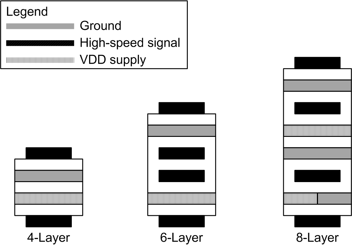
To meet signal integrity and performance requirements, at minimum a 4-layer PCB should be used. However a 6-layer board is recommended. See Figure 10-3 for the recommended layer stack ups for 4, 6, and 8-layer boards. These are recommendations not requirements, other configurations can be used as per system requirements.
 Figure 10-3 Recommended Layer Stack Up
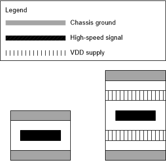
Within a PCB, it may be desirable to run traces using different methods, microstrip vs. stripline, depending on the location of the signal on the PCB. For example, it may be desirable to change layer stacking where an isolated chassis ground plane is used. Figure 10-4 shows alternative PCB stacking options.
 Figure 10-4 Alternative Layer Stack Up