JAJSLL2B April   2021  – November 2021 DP83561-SP

PRODUCTION DATA  

  1. 特長
  2. アプリケーション
  3. 概要
  4. Revision History
  5. Pin Configuration and Functions
    1. 5.1 Pin States
  6. Specifications
    1. 6.1 Absolute Maximum Ratings
    2. 6.2 ESD Ratings
    3. 6.3 Recommended Operating Conditions
    4. 6.4 Thermal Information
    5. 6.5 Electrical Characteristics
    6. 6.6 Timing Requirements
      1. 6.6.1 Timing Requirement Diagrams
    7. 6.7 Typical Characteristics
  7. Detailed Description
    1. 7.1 Overview
      1. 7.1.1 Engineering Model (Parts With /EM Suffix)
    2. 7.2 Functional Block Diagram
    3. 7.3 Feature Description
      1. 7.3.1 Copper Ethernet
        1. 7.3.1.1 1000BASE-T
        2. 7.3.1.2 100BASE-TX
        3. 7.3.1.3 10BASE-Te
      2. 7.3.2 MAC Interfaces
        1. 7.3.2.1 Reduced GMII (RGMII)
          1. 7.3.2.1.1 RGMII-TX Requirements
          2. 7.3.2.1.2 RGMII-RX Requirements
          3. 7.3.2.1.3 1000-Mbps Mode Operation
          4. 7.3.2.1.4 1000-Mbps Mode Timing
          5. 7.3.2.1.5 10- and 100-Mbps Mode
        2. 7.3.2.2 Media Independent Interface (MII)
      3. 7.3.3 Auto-Negotiation
        1. 7.3.3.1 Speed and Duplex Selection - Priority Resolution
        2. 7.3.3.2 Master and Slave Resolution
        3. 7.3.3.3 Pause and Asymmetrical Pause Resolution
        4. 7.3.3.4 Next Page Support
        5. 7.3.3.5 Parallel Detection
        6. 7.3.3.6 Restart Auto-Negotiation
        7. 7.3.3.7 Enabling Auto-Negotiation Through Software
        8. 7.3.3.8 Auto-Negotiation Complete Time
        9. 7.3.3.9 Auto-MDIX Resolution
      4. 7.3.4 Speed Optimization
      5. 7.3.5 Radiation Performance
        1. 7.3.5.1 Total Ionizing Dose (TID)
        2. 7.3.5.2 Single-Event Effects (SEE)
        3. 7.3.5.3 Single Event Functional Interrupt (SEFI) Monitor Suite
          1. 7.3.5.3.1 PCS State Machine Monitors
          2. 7.3.5.3.2 Configuration Register Monitors
          3. 7.3.5.3.3 Temperature Monitor
          4. 7.3.5.3.4 PLL Lock Monitor
      6. 7.3.6 WoL (Wake-on-LAN) Packet Detection
        1. 7.3.6.1 Magic Packet Structure
        2. 7.3.6.2 Magic Packet Example
        3. 7.3.6.3 Wake-on-LAN Configuration and Status
      7. 7.3.7 Start of Frame Detect for IEEE 1588 Time Stamp
        1. 7.3.7.1 SFD Latency Variation and Determinism
          1. 7.3.7.1.1 1000M SFD Variation in Master Mode
          2. 7.3.7.1.2 1000M SFD Variation in Slave Mode
          3. 7.3.7.1.3 100M SFD Variation
      8. 7.3.8 Cable Diagnostics
        1. 7.3.8.1 TDR
        2. 7.3.8.2 Fast Link Drop
        3. 7.3.8.3 Fast Link Detect
        4. 7.3.8.4 Energy Detect
        5. 7.3.8.5 IEEE 802.3 Test Modes
        6. 7.3.8.6 Jumbo Frames
      9. 7.3.9 Clock Output
    4. 7.4 Device Functional Modes
      1. 7.4.1 Mirror Mode
      2. 7.4.2 Loopback Mode
        1. 7.4.2.1 Near-End Loopback
          1. 7.4.2.1.1 MII Loopback
          2. 7.4.2.1.2 PCS Loopback
          3. 7.4.2.1.3 Digital Loopback
          4. 7.4.2.1.4 Analog Loopback
          5. 7.4.2.1.5 External Loopback
          6. 7.4.2.1.6 Far-End (Reverse) Loopback
        2. 7.4.2.2 Loopback Availability Exception
      3. 7.4.3 Power-Saving Modes
        1. 7.4.3.1 IEEE Power Down
        2. 7.4.3.2 Deep Power-Down Mode
        3. 7.4.3.3 Active Sleep
        4. 7.4.3.4 Passive Sleep
    5. 7.5 Programming
      1. 7.5.1 Serial Management Interface
        1. 7.5.1.1 Extended Address Space Access
          1. 7.5.1.1.1 Write Address Operation
          2. 7.5.1.1.2 Read Address Operation
          3. 7.5.1.1.3 Write (No Post Increment) Operation
          4. 7.5.1.1.4 Read (No Post Increment) Operation
          5. 7.5.1.1.5 Write (Post Increment) Operation
          6. 7.5.1.1.6 Read (Post Increment) Operation
          7. 7.5.1.1.7 Example of Read Operation Using Indirect Register Access
          8. 7.5.1.1.8 Example of Write Operation Using Indirect Register Access
      2. 7.5.2 Interrupt
      3. 7.5.3 BIST Configuration
      4. 7.5.4 Strap Configuration
      5. 7.5.5 LED Configuration
      6. 7.5.6 LED Operation From 1.8-V I/O VDD Supply
      7. 7.5.7 Reset Operation
        1. 7.5.7.1 Hardware Reset
        2. 7.5.7.2 IEEE Software Reset
        3. 7.5.7.3 Global Software Reset
        4. 7.5.7.4 Global Software Restart
        5. 7.5.7.5 PCS Restart
    6. 7.6 Register Maps
      1. 7.6.1 DP83561SP Registers
  8. Application and Implementation
    1. 8.1 Application Information
    2. 8.2 Typical Application
      1. 8.2.1 Design Requirements
      2. 8.2.2 Detailed Design Procedure
        1. 8.2.2.1 Clock Input
          1. 8.2.2.1.1 Crystal Recommendations
          2. 8.2.2.1.2 External Clock Source Recommendations
        2. 8.2.2.2 MAC Interface
          1. 8.2.2.2.1 RGMII Layout Guidelines
          2. 8.2.2.2.2 MII Layout Guidelines
        3. 8.2.2.3 Media Dependent Interface (MDI)
          1. 8.2.2.3.1 MDI Layout Guidelines
        4. 8.2.2.4 Magnetics Requirements
          1. 8.2.2.4.1 Magnetics Connection
  9. Power Supply Recommendations
    1. 9.1 Two-Supply Configuration
    2. 9.2 Three-Supply Configuration
  10. 10Layout
    1. 10.1 Layout Guidelines
      1. 10.1.1 Signal Traces
      2. 10.1.2 Return Path
      3. 10.1.3 Transformer Layout
      4. 10.1.4 Metal Pour
      5. 10.1.5 PCB Layer Stacking
    2. 10.2 Layout Example
  11. 11Device and Documentation Support
    1. 11.1 Documentation Support
      1. 11.1.1 Related Documentation
    2. 11.2 Receiving Notification of Documentation Updates
    3. 11.3 サポート・リソース
    4. 11.4 Trademarks
    5. 11.5 Electrostatic Discharge Caution
    6. 11.6 Glossary
  12. 12Mechanical, Packaging, and Orderable Information

パッケージ・オプション

メカニカル・データ(パッケージ|ピン)
サーマルパッド・メカニカル・データ
発注情報

Signal Traces

PCB traces are lossy and long traces can degrade the signal quality. Traces must be kept short as possible. Unless mentioned otherwise, all signal traces should be 50-Ω single-ended impedance. Differential traces should be 50-Ω single-ended and 100-Ω differential. Take care that the impedance is constant throughout. Impedance discontinuities cause reflections leading to EMI & signal integrity problems. Stubs must be avoided on all signal traces, especially the differential signal pairs. See Figure 10-1.

Within the differential pairs, the trace lengths must run parallel to each other and matched in length. Matched lengths minimize delay differences, avoiding an increase in common-mode noise and increased EMI.

Length matching is also important on MAC interface. All Transmit signal trace lengths must match to each other and all Receive signal trace lengths must match to each other.

Ideally, there should be no crossover or via on the signal paths. Vias present impedance discontinuities and should be minimized. Route an entire trace pair on a single layer if possible.
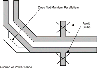
GUID-24139884-75D6-42C7-9547-0E7C2C6143E3-low.gifFigure 10-1 Avoiding Stubs in a Differential Signal Pair

Signals on different layers should not cross each other without at least one return path plane between them.

Coupling between traces is also an important factor. Unwanted coupling can cause cross talk problems. Differential pairs on the other hand, should have a constant coupling distance between them.

For convenience and efficient layout process, start by routing the critical signals first.