JAJSLL2B April   2021  – November 2021 DP83561-SP

PRODUCTION DATA  

  1. 特長
  2. アプリケーション
  3. 概要
  4. Revision History
  5. Pin Configuration and Functions
    1. 5.1 Pin States
  6. Specifications
    1. 6.1 Absolute Maximum Ratings
    2. 6.2 ESD Ratings
    3. 6.3 Recommended Operating Conditions
    4. 6.4 Thermal Information
    5. 6.5 Electrical Characteristics
    6. 6.6 Timing Requirements
      1. 6.6.1 Timing Requirement Diagrams
    7. 6.7 Typical Characteristics
  7. Detailed Description
    1. 7.1 Overview
      1. 7.1.1 Engineering Model (Parts With /EM Suffix)
    2. 7.2 Functional Block Diagram
    3. 7.3 Feature Description
      1. 7.3.1 Copper Ethernet
        1. 7.3.1.1 1000BASE-T
        2. 7.3.1.2 100BASE-TX
        3. 7.3.1.3 10BASE-Te
      2. 7.3.2 MAC Interfaces
        1. 7.3.2.1 Reduced GMII (RGMII)
          1. 7.3.2.1.1 RGMII-TX Requirements
          2. 7.3.2.1.2 RGMII-RX Requirements
          3. 7.3.2.1.3 1000-Mbps Mode Operation
          4. 7.3.2.1.4 1000-Mbps Mode Timing
          5. 7.3.2.1.5 10- and 100-Mbps Mode
        2. 7.3.2.2 Media Independent Interface (MII)
      3. 7.3.3 Auto-Negotiation
        1. 7.3.3.1 Speed and Duplex Selection - Priority Resolution
        2. 7.3.3.2 Master and Slave Resolution
        3. 7.3.3.3 Pause and Asymmetrical Pause Resolution
        4. 7.3.3.4 Next Page Support
        5. 7.3.3.5 Parallel Detection
        6. 7.3.3.6 Restart Auto-Negotiation
        7. 7.3.3.7 Enabling Auto-Negotiation Through Software
        8. 7.3.3.8 Auto-Negotiation Complete Time
        9. 7.3.3.9 Auto-MDIX Resolution
      4. 7.3.4 Speed Optimization
      5. 7.3.5 Radiation Performance
        1. 7.3.5.1 Total Ionizing Dose (TID)
        2. 7.3.5.2 Single-Event Effects (SEE)
        3. 7.3.5.3 Single Event Functional Interrupt (SEFI) Monitor Suite
          1. 7.3.5.3.1 PCS State Machine Monitors
          2. 7.3.5.3.2 Configuration Register Monitors
          3. 7.3.5.3.3 Temperature Monitor
          4. 7.3.5.3.4 PLL Lock Monitor
      6. 7.3.6 WoL (Wake-on-LAN) Packet Detection
        1. 7.3.6.1 Magic Packet Structure
        2. 7.3.6.2 Magic Packet Example
        3. 7.3.6.3 Wake-on-LAN Configuration and Status
      7. 7.3.7 Start of Frame Detect for IEEE 1588 Time Stamp
        1. 7.3.7.1 SFD Latency Variation and Determinism
          1. 7.3.7.1.1 1000M SFD Variation in Master Mode
          2. 7.3.7.1.2 1000M SFD Variation in Slave Mode
          3. 7.3.7.1.3 100M SFD Variation
      8. 7.3.8 Cable Diagnostics
        1. 7.3.8.1 TDR
        2. 7.3.8.2 Fast Link Drop
        3. 7.3.8.3 Fast Link Detect
        4. 7.3.8.4 Energy Detect
        5. 7.3.8.5 IEEE 802.3 Test Modes
        6. 7.3.8.6 Jumbo Frames
      9. 7.3.9 Clock Output
    4. 7.4 Device Functional Modes
      1. 7.4.1 Mirror Mode
      2. 7.4.2 Loopback Mode
        1. 7.4.2.1 Near-End Loopback
          1. 7.4.2.1.1 MII Loopback
          2. 7.4.2.1.2 PCS Loopback
          3. 7.4.2.1.3 Digital Loopback
          4. 7.4.2.1.4 Analog Loopback
          5. 7.4.2.1.5 External Loopback
          6. 7.4.2.1.6 Far-End (Reverse) Loopback
        2. 7.4.2.2 Loopback Availability Exception
      3. 7.4.3 Power-Saving Modes
        1. 7.4.3.1 IEEE Power Down
        2. 7.4.3.2 Deep Power-Down Mode
        3. 7.4.3.3 Active Sleep
        4. 7.4.3.4 Passive Sleep
    5. 7.5 Programming
      1. 7.5.1 Serial Management Interface
        1. 7.5.1.1 Extended Address Space Access
          1. 7.5.1.1.1 Write Address Operation
          2. 7.5.1.1.2 Read Address Operation
          3. 7.5.1.1.3 Write (No Post Increment) Operation
          4. 7.5.1.1.4 Read (No Post Increment) Operation
          5. 7.5.1.1.5 Write (Post Increment) Operation
          6. 7.5.1.1.6 Read (Post Increment) Operation
          7. 7.5.1.1.7 Example of Read Operation Using Indirect Register Access
          8. 7.5.1.1.8 Example of Write Operation Using Indirect Register Access
      2. 7.5.2 Interrupt
      3. 7.5.3 BIST Configuration
      4. 7.5.4 Strap Configuration
      5. 7.5.5 LED Configuration
      6. 7.5.6 LED Operation From 1.8-V I/O VDD Supply
      7. 7.5.7 Reset Operation
        1. 7.5.7.1 Hardware Reset
        2. 7.5.7.2 IEEE Software Reset
        3. 7.5.7.3 Global Software Reset
        4. 7.5.7.4 Global Software Restart
        5. 7.5.7.5 PCS Restart
    6. 7.6 Register Maps
      1. 7.6.1 DP83561SP Registers
  8. Application and Implementation
    1. 8.1 Application Information
    2. 8.2 Typical Application
      1. 8.2.1 Design Requirements
      2. 8.2.2 Detailed Design Procedure
        1. 8.2.2.1 Clock Input
          1. 8.2.2.1.1 Crystal Recommendations
          2. 8.2.2.1.2 External Clock Source Recommendations
        2. 8.2.2.2 MAC Interface
          1. 8.2.2.2.1 RGMII Layout Guidelines
          2. 8.2.2.2.2 MII Layout Guidelines
        3. 8.2.2.3 Media Dependent Interface (MDI)
          1. 8.2.2.3.1 MDI Layout Guidelines
        4. 8.2.2.4 Magnetics Requirements
          1. 8.2.2.4.1 Magnetics Connection
  9. Power Supply Recommendations
    1. 9.1 Two-Supply Configuration
    2. 9.2 Three-Supply Configuration
  10. 10Layout
    1. 10.1 Layout Guidelines
      1. 10.1.1 Signal Traces
      2. 10.1.2 Return Path
      3. 10.1.3 Transformer Layout
      4. 10.1.4 Metal Pour
      5. 10.1.5 PCB Layer Stacking
    2. 10.2 Layout Example
  11. 11Device and Documentation Support
    1. 11.1 Documentation Support
      1. 11.1.1 Related Documentation
    2. 11.2 Receiving Notification of Documentation Updates
    3. 11.3 サポート・リソース
    4. 11.4 Trademarks
    5. 11.5 Electrostatic Discharge Caution
    6. 11.6 Glossary
  12. 12Mechanical, Packaging, and Orderable Information

パッケージ・オプション

メカニカル・データ(パッケージ|ピン)
サーマルパッド・メカニカル・データ
発注情報
10- and 100-Mbps Mode

When the RGMII interface is operating in the 100-Mbps mode, the Ethernet Media Independent Interface (MII) is implemented by reducing the clock rate to 25 MHz. For 10-Mbps operation, the clock is further reduced to 2.5 MHz. In the RGMII 10/100 mode, the transmit clock RGMII TX_CLK is generated by the MAC and the receive clock RGMII RX_CLK is generated by the PHY. During the packet receiving operation, the RGMII RX_CLK may be stretched on either the positive or negative pulse to accommodate the transition from the free-running clock to a data synchronous clock domain. When the speed of the PHY changes, a similar stretching of the positive or negative pulses is allowed. No glitch is allowed on the clock signals during clock speed transitions.

This interface operates at 10- and 100-Mbps speeds the same way it does at 1000-Mbps mode with the exception that the data may be duplicated on the falling edge of the appropriate clock.

The MAC holds the RGMII TX_CLK low until it has ensured that it is operating at the same speed as the PHY.
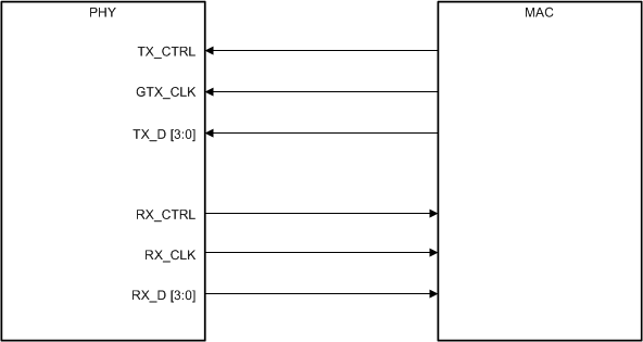
GUID-F83071B0-BF75-433E-9B50-7A03265B864C-low.gifFigure 7-4 RGMII Connections