JAJSLL2B April   2021  – November 2021 DP83561-SP

PRODUCTION DATA  

  1. 特長
  2. アプリケーション
  3. 概要
  4. Revision History
  5. Pin Configuration and Functions
    1. 5.1 Pin States
  6. Specifications
    1. 6.1 Absolute Maximum Ratings
    2. 6.2 ESD Ratings
    3. 6.3 Recommended Operating Conditions
    4. 6.4 Thermal Information
    5. 6.5 Electrical Characteristics
    6. 6.6 Timing Requirements
      1. 6.6.1 Timing Requirement Diagrams
    7. 6.7 Typical Characteristics
  7. Detailed Description
    1. 7.1 Overview
      1. 7.1.1 Engineering Model (Parts With /EM Suffix)
    2. 7.2 Functional Block Diagram
    3. 7.3 Feature Description
      1. 7.3.1 Copper Ethernet
        1. 7.3.1.1 1000BASE-T
        2. 7.3.1.2 100BASE-TX
        3. 7.3.1.3 10BASE-Te
      2. 7.3.2 MAC Interfaces
        1. 7.3.2.1 Reduced GMII (RGMII)
          1. 7.3.2.1.1 RGMII-TX Requirements
          2. 7.3.2.1.2 RGMII-RX Requirements
          3. 7.3.2.1.3 1000-Mbps Mode Operation
          4. 7.3.2.1.4 1000-Mbps Mode Timing
          5. 7.3.2.1.5 10- and 100-Mbps Mode
        2. 7.3.2.2 Media Independent Interface (MII)
      3. 7.3.3 Auto-Negotiation
        1. 7.3.3.1 Speed and Duplex Selection - Priority Resolution
        2. 7.3.3.2 Master and Slave Resolution
        3. 7.3.3.3 Pause and Asymmetrical Pause Resolution
        4. 7.3.3.4 Next Page Support
        5. 7.3.3.5 Parallel Detection
        6. 7.3.3.6 Restart Auto-Negotiation
        7. 7.3.3.7 Enabling Auto-Negotiation Through Software
        8. 7.3.3.8 Auto-Negotiation Complete Time
        9. 7.3.3.9 Auto-MDIX Resolution
      4. 7.3.4 Speed Optimization
      5. 7.3.5 Radiation Performance
        1. 7.3.5.1 Total Ionizing Dose (TID)
        2. 7.3.5.2 Single-Event Effects (SEE)
        3. 7.3.5.3 Single Event Functional Interrupt (SEFI) Monitor Suite
          1. 7.3.5.3.1 PCS State Machine Monitors
          2. 7.3.5.3.2 Configuration Register Monitors
          3. 7.3.5.3.3 Temperature Monitor
          4. 7.3.5.3.4 PLL Lock Monitor
      6. 7.3.6 WoL (Wake-on-LAN) Packet Detection
        1. 7.3.6.1 Magic Packet Structure
        2. 7.3.6.2 Magic Packet Example
        3. 7.3.6.3 Wake-on-LAN Configuration and Status
      7. 7.3.7 Start of Frame Detect for IEEE 1588 Time Stamp
        1. 7.3.7.1 SFD Latency Variation and Determinism
          1. 7.3.7.1.1 1000M SFD Variation in Master Mode
          2. 7.3.7.1.2 1000M SFD Variation in Slave Mode
          3. 7.3.7.1.3 100M SFD Variation
      8. 7.3.8 Cable Diagnostics
        1. 7.3.8.1 TDR
        2. 7.3.8.2 Fast Link Drop
        3. 7.3.8.3 Fast Link Detect
        4. 7.3.8.4 Energy Detect
        5. 7.3.8.5 IEEE 802.3 Test Modes
        6. 7.3.8.6 Jumbo Frames
      9. 7.3.9 Clock Output
    4. 7.4 Device Functional Modes
      1. 7.4.1 Mirror Mode
      2. 7.4.2 Loopback Mode
        1. 7.4.2.1 Near-End Loopback
          1. 7.4.2.1.1 MII Loopback
          2. 7.4.2.1.2 PCS Loopback
          3. 7.4.2.1.3 Digital Loopback
          4. 7.4.2.1.4 Analog Loopback
          5. 7.4.2.1.5 External Loopback
          6. 7.4.2.1.6 Far-End (Reverse) Loopback
        2. 7.4.2.2 Loopback Availability Exception
      3. 7.4.3 Power-Saving Modes
        1. 7.4.3.1 IEEE Power Down
        2. 7.4.3.2 Deep Power-Down Mode
        3. 7.4.3.3 Active Sleep
        4. 7.4.3.4 Passive Sleep
    5. 7.5 Programming
      1. 7.5.1 Serial Management Interface
        1. 7.5.1.1 Extended Address Space Access
          1. 7.5.1.1.1 Write Address Operation
          2. 7.5.1.1.2 Read Address Operation
          3. 7.5.1.1.3 Write (No Post Increment) Operation
          4. 7.5.1.1.4 Read (No Post Increment) Operation
          5. 7.5.1.1.5 Write (Post Increment) Operation
          6. 7.5.1.1.6 Read (Post Increment) Operation
          7. 7.5.1.1.7 Example of Read Operation Using Indirect Register Access
          8. 7.5.1.1.8 Example of Write Operation Using Indirect Register Access
      2. 7.5.2 Interrupt
      3. 7.5.3 BIST Configuration
      4. 7.5.4 Strap Configuration
      5. 7.5.5 LED Configuration
      6. 7.5.6 LED Operation From 1.8-V I/O VDD Supply
      7. 7.5.7 Reset Operation
        1. 7.5.7.1 Hardware Reset
        2. 7.5.7.2 IEEE Software Reset
        3. 7.5.7.3 Global Software Reset
        4. 7.5.7.4 Global Software Restart
        5. 7.5.7.5 PCS Restart
    6. 7.6 Register Maps
      1. 7.6.1 DP83561SP Registers
  8. Application and Implementation
    1. 8.1 Application Information
    2. 8.2 Typical Application
      1. 8.2.1 Design Requirements
      2. 8.2.2 Detailed Design Procedure
        1. 8.2.2.1 Clock Input
          1. 8.2.2.1.1 Crystal Recommendations
          2. 8.2.2.1.2 External Clock Source Recommendations
        2. 8.2.2.2 MAC Interface
          1. 8.2.2.2.1 RGMII Layout Guidelines
          2. 8.2.2.2.2 MII Layout Guidelines
        3. 8.2.2.3 Media Dependent Interface (MDI)
          1. 8.2.2.3.1 MDI Layout Guidelines
        4. 8.2.2.4 Magnetics Requirements
          1. 8.2.2.4.1 Magnetics Connection
  9. Power Supply Recommendations
    1. 9.1 Two-Supply Configuration
    2. 9.2 Three-Supply Configuration
  10. 10Layout
    1. 10.1 Layout Guidelines
      1. 10.1.1 Signal Traces
      2. 10.1.2 Return Path
      3. 10.1.3 Transformer Layout
      4. 10.1.4 Metal Pour
      5. 10.1.5 PCB Layer Stacking
    2. 10.2 Layout Example
  11. 11Device and Documentation Support
    1. 11.1 Documentation Support
      1. 11.1.1 Related Documentation
    2. 11.2 Receiving Notification of Documentation Updates
    3. 11.3 サポート・リソース
    4. 11.4 Trademarks
    5. 11.5 Electrostatic Discharge Caution
    6. 11.6 Glossary
  12. 12Mechanical, Packaging, and Orderable Information

パッケージ・オプション

メカニカル・データ(パッケージ|ピン)
サーマルパッド・メカニカル・データ
発注情報

LED Configuration

The DP83561-SP supports four configurable Light Emitting Diode (LED) pins: LED_0, LED_1, LED_2, and RXD7/GPIO. Several functions can be multiplexed onto the LEDs for different modes of operation. The LED operation mode can be selected using the LEDCR1 register (address 0x0018).

Because the LED output pins are also used as straps, the external components required for strapping and LED usage must be considered to avoid contention. Specifically, when the LED outputs are used to drive LEDs directly, the active state of each output driver is dependent on the logic level sampled by the corresponding AN input upon power up or reset.

If a given strap input is resistively pulled low then the corresponding output is configured as an active high driver. In the context of the 4-level straps, this occurs for modes 1, 2, and 3. Conversely, if a given strap input is resistively pulled high, then the corresponding output is configured as an active low driver. In the context of the 4-level straps, this occurs only for mode 4.

Refer to Figure 7-15 for an example of strap connections to external components. In this example, the strapping results in Mode 1 for LED_0 and Mode 4 for LED_1.

The adaptive nature of the LED outputs helps to simplify potential implementation issues of these dual-purpose pins.
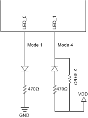
GUID-EB657B88-20CD-41FD-AC07-2C0E38D8FECC-low.gifFigure 7-15 Example Strap Connections