SNOSAY8F September 2007 – April 2015 DP83640
PRODUCTION DATA.
- 1Device Overview
- 2Revision History
-
3Pin Configuration and Functions
- 3.1 Pin Layout
- 3.2 Package Pin Assignments
- 3.3 Serial Management Interface (SMI)
- 3.4 MAC Data Interface
- 3.5 Clock Interface
- 3.6 LED Interface
- 3.7 IEEE 1588 Event/Trigger/Clock Interface
- 3.8 JTAG Interface
- 3.9 Reset and Power Down
- 3.10 Strap Options
- 3.11 10 Mb/s and 100 Mb/s PMD Interface
- 3.12 Power Supply Pins
- 4Specifications
-
5Detailed Description
- 5.1 Overview
- 5.2 Functional Block Diagram
- 5.3
Feature Description
- 5.3.1 Media Configuration
- 5.3.2 Auto-Negotiation
- 5.3.3 Auto-MDIX
- 5.3.4 LED Interface
- 5.3.5 Internal Loopback
- 5.3.6 Power Down/Interrupt
- 5.3.7 Energy Detect Mode
- 5.3.8 Link Diagnostic Capabilities
- 5.3.9 BIST
- 5.4 Device Functional Modes
- 5.5
Programming
- 5.5.1
Architecture
- 5.5.1.1 100BASE-TX Transmitter
- 5.5.1.2
100BASE-TX Receiver
- 5.5.1.2.1 Analog Front End
- 5.5.1.2.2 Digital Signal Processor
- 5.5.1.2.3 Signal Detect
- 5.5.1.2.4 MLT-3 to Binary Decoder
- 5.5.1.2.5 Clock Recovery Module
- 5.5.1.2.6 NRZI to NRZ Decoder
- 5.5.1.2.7 Serial-to-Parallel
- 5.5.1.2.8 Descrambler
- 5.5.1.2.9 Code-Group Alignment
- 5.5.1.2.10 4B/5B Decoder
- 5.5.1.2.11 100BASE-TX Link Integrity Monitor
- 5.5.1.2.12 Bad SSD Detection
- 5.5.1.3 100BASE-FX Operation
- 5.5.1.4
10BASE-T Transceiver Module
- 5.5.1.4.1 Operational Modes
- 5.5.1.4.2 Smart Squelch
- 5.5.1.4.3 Collision Detection and SQE
- 5.5.1.4.4 Carrier Sense
- 5.5.1.4.5 Normal Link Pulse Detection/Generation
- 5.5.1.4.6 Jabber Function
- 5.5.1.4.7 Automatic Link Polarity Detection and Correction
- 5.5.1.4.8 Transmit and Receive Filtering
- 5.5.1.4.9 Transmitter
- 5.5.1.4.10 Receiver
- 5.5.1
Architecture
- 5.6
Memory
- 5.6.1
Register Block
- 5.6.1.1
Register Definition
- 5.6.1.1.1 Basic Mode Control Register (BMCR)
- 5.6.1.1.2 Basic Mode Status Register (BMSR)
- 5.6.1.1.3 PHY Identifier Register #1 (PHYIDR1)
- 5.6.1.1.4 PHY Identifier Register #2 (PHYIDR2)
- 5.6.1.1.5 Auto-Negotiation Advertisement Register (ANAR)
- 5.6.1.1.6 Auto-Negotiation Link Partner Ability Register (ANLPAR) (BASE Page)
- 5.6.1.1.7 Auto-Negotiation Link Partner Ability Register (ANLPAR) (Next Page)
- 5.6.1.1.8 Auto-Negotiate Expansion Register (ANER)
- 5.6.1.1.9 Auto-Negotiation Next Page Transmit Register (ANNPTR)
- 5.6.1.1.10 PHY Status Register (PHYSTS)
- 5.6.1.1.11 MII Interrupt Control Register (MICR)
- 5.6.1.1.12 MII Interrupt Status and Event Control Register (MISR)
- 5.6.1.1.13 Page Select Register (PAGESEL)
- 5.6.1.2
Extended Registers - Page 0
- 5.6.1.2.1 False Carrier Sense Counter Register (FCSCR)
- 5.6.1.2.2 Receiver Error Counter Register (RECR)
- 5.6.1.2.3 100 Mb/s PCS Configuration and Status Register (PCSR)
- 5.6.1.2.4 RMII and Bypass Register (RBR)
- 5.6.1.2.5 LED Direct Control Register (LEDCR)
- 5.6.1.2.6 PHY Control Register (PHYCR)
- 5.6.1.2.7 10Base-T Status/Control Register (10BTSCR)
- 5.6.1.2.8 CD Test and BIST Extensions Register (CDCTRL1)
- 5.6.1.2.9 PHY Control Register 2 (PHYCR2)
- 5.6.1.2.10 Energy Detect Control (EDCR)
- 5.6.1.2.11 PHY Control Frames Configuration Register (PCFCR)
- 5.6.1.3 Test Registers - Page 1
- 5.6.1.4
Link Diagnostics Registers - Page 2
- 5.6.1.4.1 100 Mb Length Detect Register (LEN100_DET), Page 2
- 5.6.1.4.2 100 Mb Frequency Offset Indication Register (FREQ100), Page 2
- 5.6.1.4.3 TDR Control Register (TDR_CTRL), Page 2
- 5.6.1.4.4 TDR Window Register (TDR_WIN), Page 2
- 5.6.1.4.5 TDR Peak Register (TDR_PEAK), Page 2
- 5.6.1.4.6 TDR Threshold Register (TDR_THR), Page 2
- 5.6.1.4.7 Variance Control Register (VAR_CTRL), Page 2
- 5.6.1.4.8 Variance Data Register (VAR_DATA), Page 2
- 5.6.1.4.9 Link Quality Monitor Register (LQMR), Page 2
- 5.6.1.4.10 Link Quality Data Register (LQDR), Page 2
- 5.6.1.4.11 Link Quality Monitor Register 2 (LQMR2), Page 2
- 5.6.1.5
PTP 1588 Base Registers - Page 4
- 5.6.1.5.1 PTP Control Register (PTP_CTL), Page 4
- 5.6.1.5.2 PTP Time Data Register (PTP_TDR), Page 4
- 5.6.1.5.3 PTP Status Register (PTP_STS), Page 4
- 5.6.1.5.4 PTP Trigger Status Register (PTP_TSTS), Page 4
- 5.6.1.5.5 PTP Rate Low Register (PTP_RATEL), Page 4
- 5.6.1.5.6 PTP Rate High Register (PTP_RATEH), Page 4
- 5.6.1.5.7 PTP Read Checksum (PTP_RDCKSUM), Page 4
- 5.6.1.5.8 PTP Write Checksum (PTP_WRCKSUM), Page 4
- 5.6.1.5.9 PTP Transmit Timestamp Register (PTP_TXTS), Page 4
- 5.6.1.5.10 PTP Receive Timestamp Register (PTP_RXTS), Page 4
- 5.6.1.5.11 PTP Event Status Register (PTP_ESTS), Page 4
- 5.6.1.5.12 PTP Event Data Register (PTP_EDATA), Page 4
- 5.6.1.6
PTP 1588 Configuration Registers - Page 5
- 5.6.1.6.1 PTP Trigger Configuration Register (PTP_TRIG), Page 5
- 5.6.1.6.2 PTP Event Configuration Register (PTP_EVNT), Page 5
- 5.6.1.6.3 PTP Transmit Configuration Register 0 (PTP_TXCFG0), Page 5
- 5.6.1.6.4 PTP Transmit Configuration Register 1 (PTP_TXCFG1), Page 5
- 5.6.1.6.5 PHY Status Frame Configuration Register 0 (PSF_CFG0), Page 5
- 5.6.1.6.6 PTP Receive Configuration Register 0 (PTP_RXCFG0), Page 5,
- 5.6.1.6.7 PTP Receive Configuration Register 1 (PTP_RXCFG1), Page 5
- 5.6.1.6.8 PTP Receive Configuration Register 2 (PTP_RXCFG2), Page 5
- 5.6.1.6.9 PTP Receive Configuration Register 3 (PTP_RXCFG3), Page 5
- 5.6.1.6.10 PTP Receive Configuration Register 4 (PTP_RXCFG4), Page 5
- 5.6.1.6.11 PTP Temporary Rate Duration Low Register (PTP_TRDL), Page 5
- 5.6.1.6.12 PTP Temporary Rate Duration High Register (PTP_TRDH), Page 5
- 5.6.1.7
PTP 1588 Configuration Registers - Page 6
- 5.6.1.7.1 PTP Clock Output Control Register (PTP_COC), Page 6
- 5.6.1.7.2 PHY Status Frame Configuration Register 1 (PSF_CFG1), Page 6
- 5.6.1.7.3 PHY Status Frame Configuration Register 2 (PSF_CFG2), Page 6
- 5.6.1.7.4 PHY Status Frame Configuration Register 3 (PSF_CFG3), Page 6
- 5.6.1.7.5 PHY Status Frame Configuration Register 4 (PSF_CFG4), Page 6
- 5.6.1.7.6 PTP SFD Configuration Register (PTP_SFDCFG), Page 6
- 5.6.1.7.7 PTP Interrupt Control Register (PTP_INTCTL), Page 6
- 5.6.1.7.8 PTP Clock Source Register (PTP_CLKSRC), Page 6
- 5.6.1.7.9 PTP Ethernet Type Register (PTP_ETR), Page 6
- 5.6.1.7.10 PTP Offset Register (PTP_OFF), Page 6
- 5.6.1.7.11 PTP GPIO Monitor Register (PTP_GPIOMON), Page 6
- 5.6.1.7.12 PTP Receive Hash Register (PTP_RXHASH), Page 6
- 5.6.1.1
Register Definition
- 5.6.1
Register Block
-
6Application, Implementation, and Layout
- 6.1 Application Information
- 6.2 Typical Application
- 6.3 Layout
- 6.4 Power Supply Recommendations
- 7Device and Documentation Support
- 8Mechanical, Packaging, and Orderable Information
6 Application, Implementation, and Layout
NOTE
Information in the following applications sections is not part of the TI component specification, and TI does not warrant its accuracy or completeness. TI’s customers are responsible for determining suitability of components for their purposes. Customers should validate and test their design implementation to confirm system functionality.
6.1 Application Information
The DP83640 provides advanced and flexible support for IEEE 1588 for use in a highly-accurate IEEE 1588 system. It provides a 1588 digital clock implementation, IEEE 1588 Transmit and Receive packet parsing and Start-of-Frame detection, Transmit and Receive Timestamp units, trigger generation, event timestamp unit and a Pulse-Per-Second (PPS) generator.
6.1.1 Key IEEE 1588 Features
IEEE 1588 provides a time synchronization protocol, often referred to as the Precision Time Protocol (PTP), which synchronizes time across an Ethernet network. DP83640 supports IEEE 1588 Real Time Ethernet applications by providing hardware support for three time-critical elements.
- IEEE 1588 synchronized clock generation
- Packet timestamps for clock synchronization
- Event triggering and timestamping through GPIO
By combining the above capabilities, the DP83640 provides advanced and flexible support for IEEE 1588 for use in a highly-accurate IEEE 1588 system.
The DP83640 provides features for controlling the clock operation in Slave mode. The clock value can be updated to match the Master clock in several ways. In addition, the clock can be programmed to adjust its frequency to compensate for drift.
The DP83640 supports real time triggering activities and captures real time events to report to the microcontroller. Controlled devices can be connected to the DP83640 through the available GPIO.
The IEEE 1588 features are briefly presented below. For a more detailed discussion on configuring the IEEE 1588 features, refer to the Software Development Guide for the DP83640.
 Figure 6-1 DP83640 Example System Application
6.1.1.1 IEEE 1588 Synchronized Clock
The DP83640 provides several mechanisms for updating the IEEE 1588 clock based on the synchronization protocol required:
- Directly Read/Writable
- Adjustable by Add/Subtract
- Frequency Scalable
- Temporary Frequency Control
The clock consists of the following fields: Seconds (32–bit field), Nanoseconds (30–bit field), and Fractional Nanoseconds (units of 2-32 ns).
A direct set of the time value can be done by setting a new time value. A step adjustment value in nanoseconds may be added to the current value. Note that the adjustment value can be positive or negative.
The clock can be programmed to operate at an adjusted frequency value by programming a rate adjustment value. The clock can also be programmed to perform a temporary adjusted frequency value by including a rate adjustment duration. The rate adjustment allows for correction on the order of 2-32 ns per reference clock cycle. The frequency adjustment will allow the clock to correct the offset over time, avoiding any potential side-effects caused by a step adjustment in the time value.
The method used to update the clock value may depend on the difference in the values. For example, at the initial synchronization attempt, the clocks may be very far apart, and therefore require a step adjustment or a direct time set. Later, when clocks are very close in value, the temporary rate adjustment method may be the best option.
The clock does not support negative time values. If negative time is required in the system, software will have to make conversions from the PHY clock time to actual time.
The clock also does not support the upper 16-bits of the seconds field as defined by the specification (Version 2 specifies a 48-bit seconds field). If this value is required to be greater than 0, it will have to be handled by software. Because a rollover of the seconds field only occurs every 136 years, it should not be a significant burden to software.
6.1.1.1.1 IEEE 1588 Clock Output
The DP83640 provides for a synchronized clock signal for use by external devices. The output clock signal can be any frequency generated from 250 MHz divided by n, where n is an integer in the range of 2 to 255. This provides nominal frequencies from 125 MHz down to 980.4 kHz. The clock output signal is controlled by the PTP_COC register. The output clock signal is generated using the rate information in the PTP_RATE registers and is therefore frequency accurate to the 1588 clock time of the device. In addition, if clock time adjustments are made using the Temporary Rate capabilities, then all time adjustments will be tracked by the output clock signal as well. Note that any step adjustment in the 1588 clock time will not be accurately represented on the 1588 clock output signal.
6.1.1.1.2 IEEE 1588 Clock Input
The IEEE 1588 PTP logic operates on a nominal 125-MHz reference clock generated by an internal Phase Generation Module (PGM). However, options are available to use a divided-down version of the PGM clock to reduce power consumption at the expense of precision, or to use an external reference clock of up to 125 MHz in the event the 1588 clock is tracked externally.
6.1.1.2 Packet Timestamps
6.1.1.2.1 IEEE 1588 Transmit Packet Parser and Timestamp
The IEEE 1588 transmit parser monitors transmit packet data to detect IEEE 1588 Version 1 and Version 2 Event messages. The transmit parser can detect PTP Event messages transported directly in Layer2 Ethernet packets as well as in UDP/IPv4 and UDP/IPv6 packets. Upon detection of a PTP Event Message, the device will capture the transmit timestamp and provide it to software.
Because software knows the order of packet transmission, only the timestamp is recorded (there is no need to record sequence number or other information). The device can buffer four timestamps.
If enabled, an interrupt may be generated upon a Transmit Timestamp Ready.
6.1.1.2.1.1 One-Step Operation
In some cases, the transmitter can be set to operate in a One-Step mode. For Sync Messages, a One-Step device can automatically insert timestamp information in the outgoing packet. This eliminates the need for software to read the timestamp and send a follow up message.
6.1.1.2.2 IEEE 1588 Receive Packet Parser and Timestamp
The IEEE 1588 receive parser monitors receive packet data to detect IEEE 1588 Version 1 and Version 2 Event messages. The receive parser can detect PTP Event messages transported directly in Ethernet packets as well as in UDP/IPv4 and UDP/IPv6 packets. Upon detection of a PTP Event message, the device will capture the receive timestamp and provide the timestamp value to software. In addition to the timestamp, the device will record the 16-bit SequenceId, the 4-bit messageType field, and generate a 12-bit hash value for octets 20-29 of the PTP event message. The device can buffer four timestamps.
An interrupt will be generated, if enabled, upon a Receive Timestamp Ready.
6.1.1.2.2.1 Receive Timestamp Insertion
The DP83640 can deliver the timestamp to software by inserting the timestamp in the received packet. This allows for a simple method to deliver the packet to software without having to match the timestamp to the correct packet. This also eliminates the need to read the receive timestamp through the Serial Management Interface.
6.1.1.2.3 NTP Packet Timestamp
The DP83640 may be programmed to timestamp NTP packets instead of PTP packets. This operation is enabled by setting the NTP_TS_EN control in the PTP_TXCFG0 register. When configured for NTP timestamps, the DP83640 will timestamp packets with the NTP UDP port number rather than the PTP port number (note that the device cannot be configured to timestamp both PTP and NTP packets). One-Step operation is not supported for NTP timestamps, so transmit timestamps cannot be inserted directly into outgoing NTP packets. Timestamp insertion is available for receive timestamps but must use a single, fixed location.
6.1.1.3 Event Triggering and Timestamping
6.1.1.3.1 IEEE 1588 Event Triggering
The DP83640 is capable of being programmed to generate a trigger signal on an output pin based on the IEEE 1588 time value. Each trigger can be programmed to generate a one-time rising or falling edge, a single pulse of programmable width, or a periodic signal.
For each trigger, the microcontroller specifies the desired GPIO and time that the activity is to occur. The trigger is generated when the internal IEEE 1588 clock matches the desired activation time.
The device supports up to 8 trigger signals which can be output on any of the GPIO signal pins. Multiple triggers may be assigned to a single GPIO, allowing generation of more complex waveforms (that is, a sequence of varying width pulses). The trigger signals are OR’ed together to form a combined signal.
The triggers are configured through the PTP Trigger Configuration Registers. The trigger time and width settings are controlled through the PTP Control and Time Data registers.
The DP83640 can be programmed to output a Pulse-Per-Second (PPS) signal using the trigger functions.
6.1.1.3.2 IEEE 1588 Event Timestamping
The DP83640 can be programmed to timestamp an event by monitoring an input signal. The event can be monitored for rising edge, falling edge, or either. The Event Timestamp Unit can monitor up to eight events which can be set to any of the GPIO signal pins. PTP event timestamps are stored in a queue which allows storage of up to eight timestamps.
When an event timestamp is available, the device will set the EVENT_RDY bit in the PTP Status Register. The PTP Event Status Register (PTP_ESTS) provides detailed information on the next available event timestamp, including information on the event number, rise/fall direction, and indication of events missed due to overflow of the devices Event queue.
Event timestamp values should be adjusted by 35 ns (3 times period of the IEEE 1588 reference clock frequency of 125 MHz + 11 ns) to compensate for input path and synchronization delays.
The Event Timestamp Unit is configured through the PTP Event Configuration Register (PTP_EVNT).
6.1.1.4 PTP Interrupts
The PTP module may interrupt the system using the PWRDOWN/INTN pin on the device, shared with other interrupts from the PHY. As an alternative, the device may be programmed to use a GPIO pin to generate PTP interrupts separate from other PHY interrupts.
6.1.1.5 GPIO
The DP83640 features 12 IEEE 1588 GPIO pins. These GPIO pins allow for event monitoring, triggering, interrupts, and a clock output. The LED pins comprise 3 of the 12 GPIO pins. If an LED pin is to be used as a GPIO, its LED function must be disabled prior to configuring the GPIO function.
6.2 Typical Application
 Figure 6-2 Typical Application Schematic
6.2.1 Design Requirements
The design requirements for DP83640 are:
- ANA33VDD = 3.3 V
- IO_VDD = 3.3 V or 2.5 V
- Clock Input = 25 MHz for MII and 50 MHz for RMII
6.2.1.1 TPI Network Circuit
Figure 6-3 shows the recommended circuit for a 10/100 Mb/s twisted-pair interface.
Below is a partial list of recommended transformers. It is important that the user realize that variations with PCB and component characteristics requires that the application be tested to ensure that the circuit meets the requirements of the intended application.
- Pulse H1102
- Pulse H2019
- Pulse J0011D21
- Pulse J0011D21B
 Figure 6-3 10/100 Mb/s Twisted-Pair Interface
6.2.1.2 Fiber Network Circuit
Figure 6-4 shows the recommended circuit for a 100 Mb/s fiber-pair interface.
 Figure 6-4 100 Mb/s Fiber-Pair Interface
6.2.1.3 ESD Protection
Typically, ESD precautions are predominantly in effect when handling the devices or board before being installed in a system. In those cases, strict handling procedures need be implemented during the manufacturing process to greatly reduce the occurrences of catastrophic ESD events. After the system is assembled, internal components are less sensitive from ESD events.
The network interface pins are more susceptible to ESD events.
6.2.1.4 Clock In (X1) Recommendations
The DP83640 supports an external CMOS level oscillator source or a crystal resonator device.
6.2.1.4.1 Oscillator
If an external clock source is used, X1 should be tied to the clock source and X2 should be left floating.
The CMOS 25-MHz oscillator specifications for MII Mode are listed in Table 6-1. For RMII Slave Mode, the CMOS 50-MHz oscillator specifications are listed in Table 6-2. For RMII Slave mode, it is not recommended that the system clock out, Pin 24, be used as the reference clock to the MAC without first verifying the interface timing. See AN-1405 (SNLA076) for more details.
6.2.1.4.2 Crystal
A 25-MHz, parallel, 20-pF load crystal resonator should be used if a crystal source is desired. shows a typical connection for a crystal resonator circuit. The load capacitor values will vary with the crystal vendors; check with the vendor for the recommended loads.
The oscillator circuit is designed to drive a parallel resonance AT cut crystal with a minimum drive level of 100 µW and a maximum of 500 µW. If a crystal is specified for a lower drive level, a current limiting resistor should be placed in series between X2 and the crystal.
As a starting point for evaluating an oscillator circuit, if the requirements for the crystal are not known, CL1 and CL2 should be set at 33 pF, and R1 should be set at 0 Ω.
Specification for 25-MHz crystal are listed in Table 6-3.
 Crystal Oscillator Circuit
Table 6-1 25-MHz Oscillator Specification
| PARAMETER | MIN | TYP | MAX | UNITS | CONDITION |
|---|---|---|---|---|---|
| Frequency | 25 | MHz | |||
| Frequency Tolerance | ±50 | ppm | Operational Temperature | ||
| Frequency Stability | ±50 | ppm | 1 year aging | ||
| Rise / Fall Time | 6 | nsec | 20% - 80% | ||
| Jitter | 800 (1) | psec | Short term | ||
| Jitter | 800 (1) | psec | Long term | ||
| Symmetry | 40% | 60% | Duty Cycle |
Table 6-2 50-MHz Oscillator Specification
| PARAMETER | MIN | TYP | MAX | UNITS | CONDITION |
|---|---|---|---|---|---|
| Frequency | 50 | MHz | |||
| Frequency Tolerance | ±50 | ppm | Operational Temperature | ||
| Frequency Stability | ±50 | ppm | Operational Temperature | ||
| Rise / Fall Time | 6 | nsec | 20% - 80% | ||
| Jitter | 800 (1) | psec | Short term | ||
| Jitter | 800 (1) | psec | Long term | ||
| Symmetry | 40% | 60% | Duty Cycle |
Table 6-3 25-MHz Crystal Specification
| PARAMETER | MIN | TYP | MAX | UNITS | CONDITION |
|---|---|---|---|---|---|
| Frequency | 25 | MHz | |||
| Frequency Tolerance | ±50 | ppm | Operational Temperature | ||
| Frequency Stability | ±50 | ppm | 1 year aging | ||
| Shunt Capacitance | 25 | 40 | pF | Range of CL1and CL2 |
6.2.1.5 Magnetics
The magnetics have a large impact on the PHY performance as well. While several components are listed below, others may be compatible following the requirements listed in Table 6-4. It is recommended that the magnetics include both an isolation transformer and an integrated common mode choke to reduce EMI. When doing the layout, do not run signals under the magnetics. This could cause unwanted noise crosstalk. Likewise void the planes under discrete magnetics, this will help prevent common mode noise coupling. To save board space and reduce component count, an RJ-45 with integrated magnetics may be used.
Table 6-4 Magnetics Requirements
| PARAMETER | TYP | UNITS | CONDITION |
|---|---|---|---|
| Turn Ratio | 1:1 | — | ±2% |
| Insertion Loss | –1 | dB | 1-100 MHz |
| Return Loss | –16 | dB | 1-30 MHz |
| –12 | dB | 30-60 MHz | |
| 10 | dB | 60-80 MHz | |
| Differential to Common Rejection Ratio | –30 | dB | 1-50MHz |
| –20 | dB | 50-150 MHz | |
| Crosstalk | –35 | dB | 30 MHz |
| –30 | dB | 60 MHz | |
| Isolation | 1,500 | dB | HPOT |
6.2.2 Detailed Design Procedure
6.2.2.1 MAC Interface (MII/RMII)
The Media Independent Interface (MII) connects the PHYTER component to the Media Access Controller (MAC). The MAC may in fact be a discrete device, integrated into a microprocessor, CPU or FPGA. On the MII signals, the IEEE specification states the bus should be 68-Ω impedance. For space critical designs, the PHYTER family of products also support Reduced MII (RMII). For additional information on this mode of operation, refer to the AN-1405 DP83848 Single 10/100 Mb/s Ethernet Transceiver Reduced Media Independent Interface (RMII) Mode Application Report (SNLA076).
6.2.2.1.1 Termination Requirement
To reduce digital signal energy, 50-Ω series termination resistors are recommended for all MII output signals (including RXCLK, TXCLK, and RX Data signals.)
6.2.2.1.2 Recommended Maximum Trace Length
Although RMII and MII are synchronous bus architectures, there are a number of factors limiting signal trace lengths. With a longer trace, the signal becomes more attenuated at the destination and thus more susceptible to noise interference. Longer traces also act as antennas, and if run on the surface layer, can increase EMI radiation. If a long trace is running near and adjacent to a noisy signal, the unwanted signals could be coupled in as cross talk. It is recommended to keep the signal trace lengths as short as possible. Ideally, keep the traces under 6 inches. Trace length matching, to within 2.0 inches on the MII or RMII bus is also recommended. Significant differences in the trace lengths can cause data timing issues. As with any high speed data signal, good design practices dictate that impedance should be maintained and stubs should be avoided throughout the entire data path.
6.2.2.2 Calculating Impedance
The following equations can be used to calculate the differential impedance of the board. For microstrip traces, a solid ground plane is needed under the signal traces. The ground plane helps keep the EMI localized and the trace impedance continuous. Because stripline traces are typically sandwiched between the ground/supply planes, they have the advantage of lower EMI radiation and less noise coupling. The trade off of using strip line is lower propagation speed.
6.2.2.2.1 Microstrip Impedance - Single-Ended

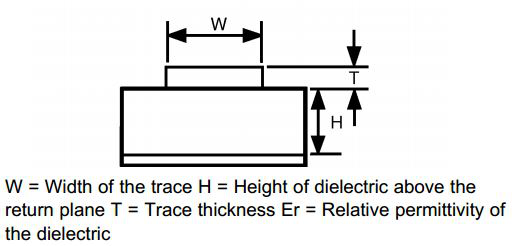 Figure 6-5 Microstrip Impedance - Single-Ended
6.2.2.2.2 Stripline Impedance – Single-Ended

 Figure 6-6 Stripline Impedance – Single-Ended
6.2.2.2.3 Microstrip Impedance - Differential

 Figure 6-7 Microstrip Impedance - Differential
6.2.2.2.4 Stripline Impedance - Differential

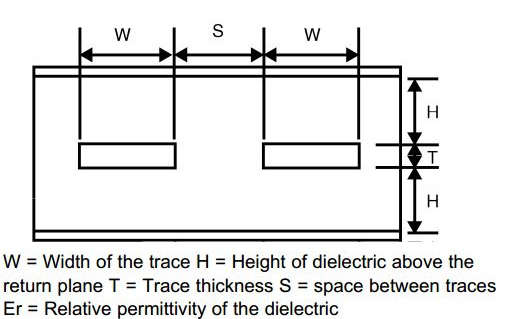 Figure 6-8 Stripline Impedance - Differential
6.2.3 Application Curves
 Figure 6-9 Sample 100 Mb/s Waveform (MLT-3)
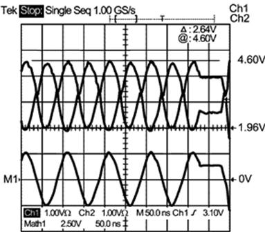 Figure 6-10 Sample 10 Mb/s Waveform
6.3 Layout
6.3.1 Layout Guidelines
6.3.1.1 PCB Layout Considerations
Place the 49.9-Ω, 1% resistors, and 0.1-μF decoupling capacitor, near the PHYTER TD± and RD± pins and via directly to the VDD plane.
Stubs should be avoided on all signal traces, especially the differential signal pairs. See Figure 6-11.
Within the pairs (for example, TD+ and TD-), the trace lengths should be run parallel to each other and matched in length. Matched lengths minimize delay differences, avoiding an increase in common mode noise and increased EMI. See Figure 6-11.
Ideally, there should be no crossover or via on the signal paths. Vias present impedance discontinuities and should be minimized. Route an entire trace pair on a single layer if possible.
PCB trace lengths should be kept as short as possible.
Signal traces should not be run such that they cross a plane split. See Figure 6-12. A signal crossing a plane split may cause unpredictable return path currents and would likely impact signal quality as well, potentially creating EMI problems.
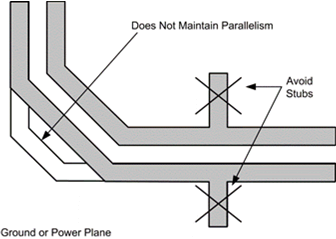 Figure 6-11 Avoiding Stubs in a Differential Signal Pair
 Figure 6-12 Differential Signal Pair-Plane Crossing
MDI signal traces should have 50 Ω to ground or 100-Ω differential controlled impedance. Many tools are available online to calculate this.
6.3.1.2 PCB Layer Stacking
To meet signal integrity and performance requirements, at minimum a four-layer PCB is recommended for implementing PHYTER components in end user systems. The following layer stack-ups are recommended for four, six, and eight-layer boards, although other options are possible.
 Figure 6-13 PCB Stripline Layer Stacking
Within a PCB, it may be desirable to run traces using different methods, microstrip vs. stripline, depending on the location of the signal on the PCB. For example, it may be desirable to change layer stacking where an isolated chassis ground plane is used. Figure 6-14 illustrates alternative PCB stacking options.
 Figure 6-14 Alternative PCB Stripline Layer Stacking
6.3.2 Layout Example
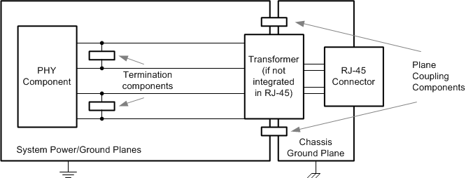 Figure 6-15 Layout Example
6.4 Power Supply Recommendations
The VDD supply pins of the device should be bypassed with low impedance 0.1-μF surface mount capacitors. To reduce EMI, the capacitors should be places as close as possible to the component VDD supply pins, preferably between the supply pins and the vias connecting to the power plane. In some systems it may be desirable to add 0-Ω resistors in series with supply pins, as the resistor pads provide flexibility if adding EMI beads becomes necessary to meet system level certification testing requirements (see Figure 6-16). It is recommended the PCB have at least one solid ground plane and one solid VDD plane to provide a low impedance power source to the component. This also provides a low impedance return path for non-differential digital MII and clock signals. A 10.0-μF capacitor should also be placed near the PHY component for local bulk bypassing between the VDD and ground planes.
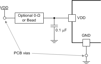 Figure 6-16 VDD Bypass Layout