JAJSC32E September 2012 – June 2019 DP83848-EP
PRODUCTION DATA.
- 1 デバイスの概要
- 2 改訂履歴
- 3 Pin Configuration and Functions
-
4 Specifications
- 4.1 Absolute Maximum Ratings
- 4.2 ESD Ratings
- 4.3 Recommended Operating Conditions
- 4.4 Thermal Information
- 4.5 DC Specifications
- 4.6
AC Specifications
- 4.6.1 Power Up Timing
- 4.6.2 Reset Timing
- 4.6.3 MII Serial Management Timing
- 4.6.4 100-Mbps MII Transmit Timing
- 4.6.5 100-Mbps MII Receive Timing
- 4.6.6 100BASE-TX Transmit Packet Latency Timing
- 4.6.7 100BASE-TX Transmit Packet Deassertion Timing
- 4.6.8 100BASE-TX Transmit Timing (tR/F and Jitter)
- 4.6.9 100BASE-TX Receive Packet Latency Timing
- 4.6.10 100BASE-TX Receive Packet Deassertion Timing
- 4.6.11 10-Mbps MII Transmit Timing
- 4.6.12 10-Mbps MII Receive Timing
- 4.6.13 10-Mbps Serial Mode Transmit Timing
- 4.6.14 10-Mbps Serial Mode Receive Timing
- 4.6.15 10BASE-T Transmit Timing (Start of Packet)
- 4.6.16 10BASE-T Transmit Timing (End of Packet)
- 4.6.17 10BASE-T Receive Timing (Start of Packet)
- 4.6.18 10BASE-T Receive Timing (End of Packet)
- 4.6.19 10-Mbps Heartbeat Timing
- 4.6.20 10-Mbps Jabber Timing
- 4.6.21 10BASE-T Normal Link Pulse Timing
- 4.6.22 Auto-Negotiation Fast Link Pulse (FLP) Timing
- 4.6.23 100BASE-TX Signal Detect Timing
- 4.6.24 100-Mbps Internal Loopback Timing
- 4.6.25 10-Mbps Internal Loopback Timing
- 4.6.26 RMII Transmit Timing
- 4.6.27 RMII Receive Timing
- 4.6.28 Isolation Timing
- 4.6.29 25MHz_OUT Timing
-
5 Detailed Description
- 5.1 Overview
- 5.2 Functional Block Diagram
- 5.3 Feature Description
- 5.4 Device Functional Modes
- 5.5
Programming
- 5.5.1
Architecture
- 5.5.1.1 100BASE-TX Transmitter
- 5.5.1.2
100BASE-TX Receiver
- 5.5.1.2.1 Analog Front End
- 5.5.1.2.2 Digital Signal Processor
- 5.5.1.2.3 Signal Detect
- 5.5.1.2.4 MLT-3 to NRZI Decoder
- 5.5.1.2.5 NRZI to NRZ
- 5.5.1.2.6 Serial to Parallel
- 5.5.1.2.7 Descrambler
- 5.5.1.2.8 Code-group Alignment
- 5.5.1.2.9 4B/5B Decoder
- 5.5.1.2.10 100BASE-TX Link Integrity Monitor
- 5.5.1.2.11 Bad SSD Detection
- 5.5.1.3
10BASE-T Transceiver Module
- 5.5.1.3.1 Operational Modes
- 5.5.1.3.2 Smart Squelch
- 5.5.1.3.3 Collision Detection and SQE
- 5.5.1.3.4 Carrier Sense
- 5.5.1.3.5 Normal Link Pulse Detection and Generation
- 5.5.1.3.6 Jabber Function
- 5.5.1.3.7 Automatic Link Polarity Detection and Correction
- 5.5.1.3.8 Transmit and Receive Filtering
- 5.5.1.3.9 Transmitter
- 5.5.1.3.10 Receiver
- 5.5.1
Architecture
- 5.6
Memory
- 5.6.1
Register Definition
- 5.6.1.1 Basic Mode Control Register (BMCR)
- 5.6.1.2 Basic Mode Status Register (BMSR)
- 5.6.1.3 PHY Identifier Register #1 (PHYIDR1)
- 5.6.1.4 PHY Identifier Register #2 (PHYIDR2)
- 5.6.1.5 Auto-Negotiation Advertisement Register (ANAR)
- 5.6.1.6 Auto-Negotiation Link Partner Ability Register (ANLPAR) (BASE Page)
- 5.6.1.7 Auto-Negotiation Link Partner Ability Register (ANLPAR) (Next Page)
- 5.6.1.8 Auto-Negotiate Expansion Register (ANER)
- 5.6.1.9 Auto-Negotiation Next Page Transmit Register (ANNPTR)
- 5.6.2
Extended Registers
- 5.6.2.1 PHY Status Register (PHYSTS)
- 5.6.2.2 MII Interrupt Control Register (MICR)
- 5.6.2.3 MII Interrupt Status and Miscellaneous Control Register (MISR)
- 5.6.2.4 False Carrier Sense Counter Register (FCSCR)
- 5.6.2.5 Receiver Error Counter Register (RECR)
- 5.6.2.6 100 Mbps PCS Configuration and Status Register (PCSR)
- 5.6.2.7 RMII and Bypass Register (RBR)
- 5.6.2.8 LED Direct Control Register (LEDCR)
- 5.6.2.9 PHY Control Register (PHYCR)
- 5.6.2.10 10Base-T Status/Control Register (10BTSCR)
- 5.6.2.11 CD Test and BIST Extensions Register (CDCTRL1)
- 5.6.2.12 Energy Detect Control (EDCR)
- 5.6.1
Register Definition
- 6 Application and Implementation
- 7 Power Supply Recommendations
- 8 Layout
- 9 デバイスおよびドキュメントのサポート
- 10メカニカル、パッケージ、および注文情報
パッケージ・オプション
メカニカル・データ(パッケージ|ピン)
サーマルパッド・メカニカル・データ
発注情報
5.5.1.3.2 Smart Squelch
The smart squelch is responsible for determining when valid data is present on the differential receive inputs. The DP83848-EP implements an intelligent receive squelch to ensure that impulse noise on the receive inputs will not be mistaken for a valid signal. Smart squelch operation is independent of the 10BASE-T operational mode.
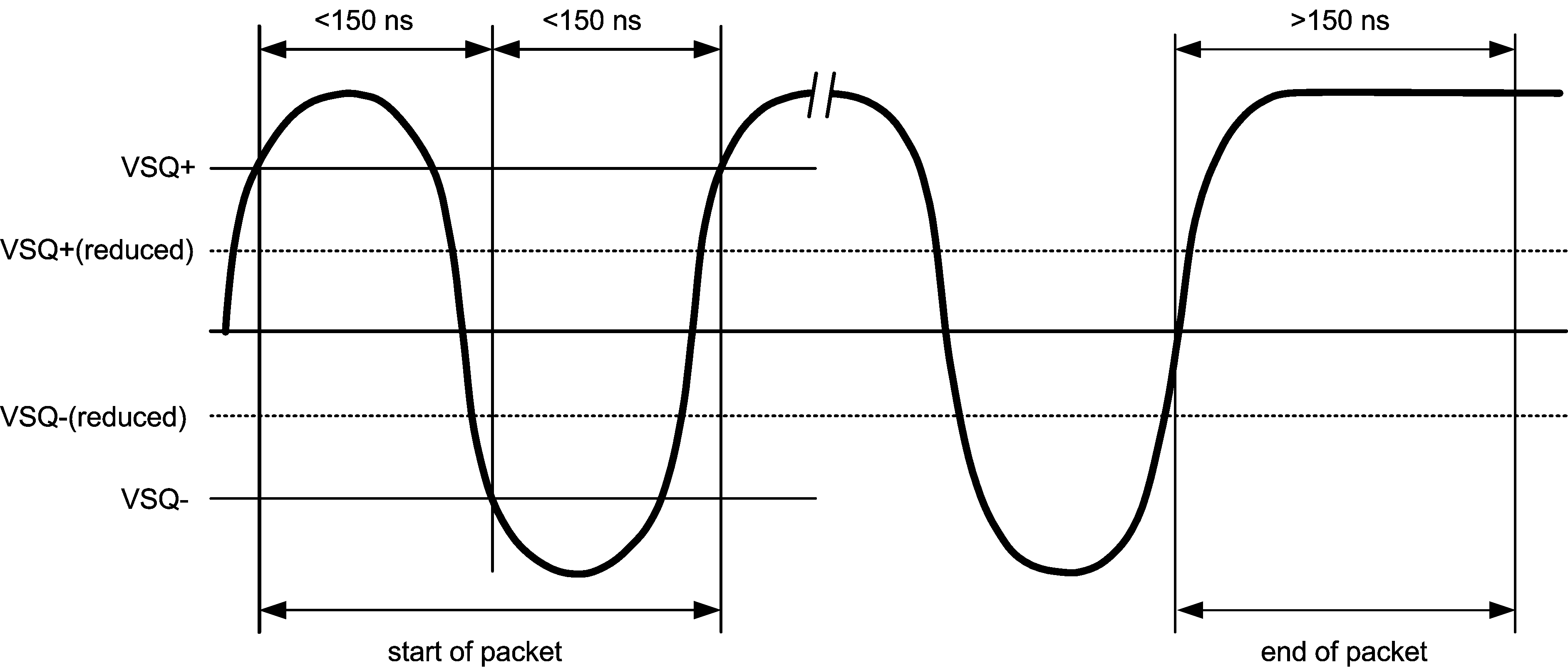
The squelch circuitry employs a combination of amplitude and timing measurements (as specified in the IEEE 802.3 10BSE-T standard) to determine the validity of data on the twisted-pair inputs (see Figure 5-9).
The signal at the start of a packet is checked by the smart squelch and any pulses not exceeding the squelch level (either positive or negative, depending upon polarity) will be rejected. Once this first squelch level is overcome correctly, the opposite squelch level must then be exceeded within 150 ns. Finally the signal must again exceed the original squelch level within 150 ns to ensure that the input waveform will not be rejected. This checking procedure results in the loss of typically three preamble bits at the beginning of each packet.
Only after all these conditions have been satisfied will a control signal be generated to indicate to the remainder of the circuitry that valid data is present. At this time, the smart squelch circuitry is reset.
Valid data is considered to be present until the squelch level has not been generated for a time longer than 150 ns, indicating the End of Packet. Once good data has been detected, the squelch levels are reduced to minimize the effect of noise causing premature End of Packet detection.
 Figure 5-9 10BASE-T Twisted-Pair Smart Squelch Operation