JAJSFD3G August 2016 – March 2019 DRA780 , DRA781 , DRA782 , DRA783 , DRA785 , DRA786 , DRA787 , DRA788
PRODUCTION DATA.
- 1デバイスの概要
- 2改訂履歴
- 3Device Comparison
-
4Terminal Configuration and Functions
- 4.1 Pin Diagram
- 4.2 Pin Attributes
- 4.3
Signal Descriptions
- 4.3.1 VIP
- 4.3.2 DSS
- 4.3.3 SD_DAC
- 4.3.4 ADC
- 4.3.5 Camera Control
- 4.3.6 CPI
- 4.3.7 CSI2
- 4.3.8 EMIF
- 4.3.9 GPMC
- 4.3.10 Timers
- 4.3.11 I2C
- 4.3.12 UART
- 4.3.13 McSPI
- 4.3.14 QSPI
- 4.3.15 McASP
- 4.3.16 DCAN and MCAN
- 4.3.17 GMAC_SW
- 4.3.18 SDIO Controller
- 4.3.19 GPIO
- 4.3.20 ePWM
- 4.3.21 ATL
- 4.3.22 Test Interfaces
- 4.3.23 System and Miscellaneous
- 4.3.24 Power Supplies
- 4.4 Pin Multiplexing
- 4.5 Connections for Unused Pins
-
5Specifications
- 5.1 Absolute Maximum Ratings
- 5.2 ESD Ratings
- 5.3 Power on Hour (POH) Limits
- 5.4 Recommended Operating Conditions
- 5.5 Operating Performance Points
- 5.6 Power Consumption Summary
- 5.7
Electrical Characteristics
- Table 5-6 LVCMOS DDR DC Electrical Characteristics
- Table 5-7 Dual Voltage LVCMOS I2C DC Electrical Characteristics
- Table 5-8 IQ1833 Buffers DC Electrical Characteristics
- Table 5-9 IHHV1833 Buffers DC Electrical Characteristics
- Table 5-10 LVCMOS Analog OSC Buffers DC Electrical Characteristics
- Table 5-11 Dual Voltage LVCMOS DC Electrical Characteristics
- Table 5-12 Analog-to-Digital ADC Subsystem Electrical Specifications
- 5.8 Thermal Characteristics
- 5.9
Timing Requirements and Switching Characteristics
- 5.9.1 Timing Parameters and Information
- 5.9.2 Interface Clock Specifications
- 5.9.3 Power Supply Sequences
- 5.9.4 Clock Specifications
- 5.9.5 Recommended Clock and Control Signal Transition Behavior
- 5.9.6
Peripherals
- 5.9.6.1 Timing Test Conditions
- 5.9.6.2 VIP
- 5.9.6.3 DSS
- 5.9.6.4 EMIF
- 5.9.6.5 GPMC
- 5.9.6.6 GP Timers
- 5.9.6.7 I2C
- 5.9.6.8 UART
- 5.9.6.9 McSPI
- 5.9.6.10 QSPI
- 5.9.6.11
McASP
- Table 5-50 Timing Requirements for McASP1
- Table 5-51 Timing Requirements for McASP2
- Table 5-52 Timing Requirements for McASP3
- Table 5-53 Switching Characteristics Over Recommended Operating Conditions for McASP1
- Table 5-54 Switching Characteristics Over Recommended Operating Conditions for McASP2
- Table 5-55 Switching Characteristics Over Recommended Operating Conditions for McASP3
- 5.9.6.12 DCAN and MCAN
- 5.9.6.13
GMAC_SW
- 5.9.6.13.1 GMAC MDIO Interface Timings
- 5.9.6.13.2
GMAC RGMII Timings
- Table 5-63 Timing Requirements for rgmiin_rxc - RGMIIn Operation
- Table 5-64 Timing Requirements for GMAC RGMIIn Input Receive for 10/100/1000 Mbps
- Table 5-65 Switching Characteristics Over Recommended Operating Conditions for rgmiin_txctl - RGMIIn Operation for 10/100/1000 Mbit/s
- Table 5-66 Switching Characteristics for GMAC RGMIIn Output Transmit for 10/100/1000 Mbps
- 5.9.6.14 SDIO Controller
- 5.9.6.15 GPIO
- 5.9.6.16 ATL
- 5.9.7
Emulation and Debug Subsystem
- 5.9.7.1
JTAG Electrical Data/Timing
- Table 5-78 Timing Requirements for IEEE 1149.1 JTAG
- Table 5-79 Switching Characteristics Over Recommended Operating Conditions for IEEE 1149.1 JTAG
- Table 5-80 Timing Requirements for IEEE 1149.1 JTAG With RTCK
- Table 5-81 Switching Characteristics Over Recommended Operating Conditions for IEEE 1149.1 JTAG With RTCK
- 5.9.7.2 Trace Port Interface Unit (TPIU)
- 5.9.7.1
JTAG Electrical Data/Timing
-
6Detailed Description
- 6.1 Description
- 6.2 Functional Block Diagram
- 6.3 DSP Subsystem
- 6.4 IPU
- 6.5 EVE
- 6.6 Memory Subsystem
- 6.7 Interprocessor Communication
- 6.8 Interrupt Controller
- 6.9 EDMA
- 6.10 Peripherals
- 6.11 On-Chip Debug
-
7Applications, Implementation, and Layout
- 7.1 Introduction
- 7.2 Power Optimizations
- 7.3 Core Power Domains
- 7.4 Single-Ended Interfaces
- 7.5 Differential Interfaces
- 7.6 Clock Routing Guidelines
- 7.7 DDR2 Board Design and Layout Guidelines
- 7.8
DDR3 Board Design and Layout Guidelines
- 7.8.1 DDR3 General Board Layout Guidelines
- 7.8.2
DDR3 Board Design and Layout Guidelines
- 7.8.2.1 Board Designs
- 7.8.2.2 DDR3 Device Combinations
- 7.8.2.3 DDR3 Interface Schematic
- 7.8.2.4 Compatible JEDEC DDR3 Devices
- 7.8.2.5 PCB Stackup
- 7.8.2.6 Placement
- 7.8.2.7 DDR3 Keepout Region
- 7.8.2.8 Bulk Bypass Capacitors
- 7.8.2.9 High-Speed Bypass Capacitors
- 7.8.2.10 Net Classes
- 7.8.2.11 DDR3 Signal Termination
- 7.8.2.12 VTT
- 7.8.2.13 CK and ADDR_CTRL Topologies and Routing Definition
- 7.8.2.14 Data Topologies and Routing Definition
- 7.8.2.15 Routing Specification
- 7.9 CVIDEO/SD-DAC Guidelines and Electrical Data/Timing
- 8Device and Documentation Support
- 9Mechanical, Packaging, and Orderable Information
パッケージ・オプション
デバイスごとのパッケージ図は、PDF版データシートをご参照ください。
メカニカル・データ(パッケージ|ピン)
- ABF|367
サーマルパッド・メカニカル・データ
発注情報
7.8.2.3.2 16-Bit DDR3 Interface
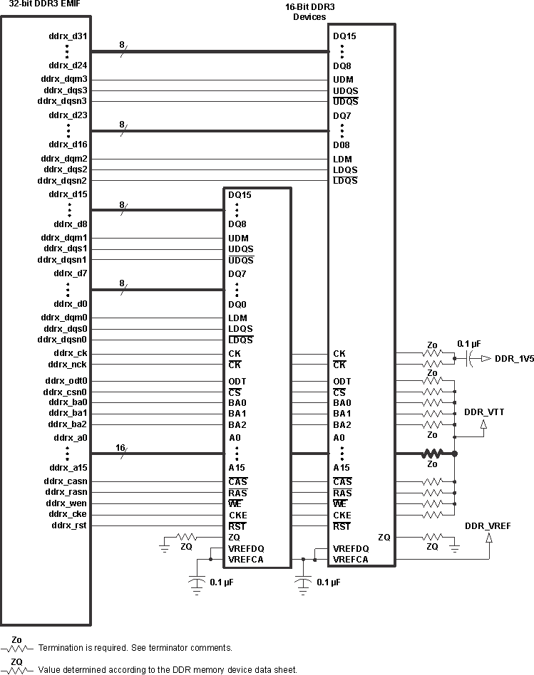
Note that the 16-bit wide interface schematic is practically identical to the 32-bit interface (see Figure 7-32); only the high-word DDR memories are removed and the unused DQS inputs are tied off.
When not using all or part of a DDR interface, the proper method of handling the unused pins is to tie off the ddrx_dqsi pins to ground via a 1k-Ω resistor and to tie off the ddrx_dqsni pins to the corresponding vdds_ddrx supply via a 1k-Ω resistor. This needs to be done for each byte not used. Although these signals have internal pullups and pulldowns, external pullups and pulldowns provide additional protection against external electrical noise causing activity on the signals.
The vdds_ddr and vdds18v_ddrx power supply pins need to be connected to their respective power supplies even if upper data byte lanes are not being used. All other DDR interface pins can be left unconnected. Note that the supported modes for use of the DDR EMIF are 32-bits wide, 16-bits wide, or not used.
 Figure 7-32 32-Bit, One-Bank DDR3 Interface Schematic Using Two 16-Bit DDR3 Devices