JAJSFD3G August 2016 – March 2019 DRA780 , DRA781 , DRA782 , DRA783 , DRA785 , DRA786 , DRA787 , DRA788
PRODUCTION DATA.
- 1デバイスの概要
- 2改訂履歴
- 3Device Comparison
-
4Terminal Configuration and Functions
- 4.1 Pin Diagram
- 4.2 Pin Attributes
- 4.3
Signal Descriptions
- 4.3.1 VIP
- 4.3.2 DSS
- 4.3.3 SD_DAC
- 4.3.4 ADC
- 4.3.5 Camera Control
- 4.3.6 CPI
- 4.3.7 CSI2
- 4.3.8 EMIF
- 4.3.9 GPMC
- 4.3.10 Timers
- 4.3.11 I2C
- 4.3.12 UART
- 4.3.13 McSPI
- 4.3.14 QSPI
- 4.3.15 McASP
- 4.3.16 DCAN and MCAN
- 4.3.17 GMAC_SW
- 4.3.18 SDIO Controller
- 4.3.19 GPIO
- 4.3.20 ePWM
- 4.3.21 ATL
- 4.3.22 Test Interfaces
- 4.3.23 System and Miscellaneous
- 4.3.24 Power Supplies
- 4.4 Pin Multiplexing
- 4.5 Connections for Unused Pins
-
5Specifications
- 5.1 Absolute Maximum Ratings
- 5.2 ESD Ratings
- 5.3 Power on Hour (POH) Limits
- 5.4 Recommended Operating Conditions
- 5.5 Operating Performance Points
- 5.6 Power Consumption Summary
- 5.7
Electrical Characteristics
- Table 5-6 LVCMOS DDR DC Electrical Characteristics
- Table 5-7 Dual Voltage LVCMOS I2C DC Electrical Characteristics
- Table 5-8 IQ1833 Buffers DC Electrical Characteristics
- Table 5-9 IHHV1833 Buffers DC Electrical Characteristics
- Table 5-10 LVCMOS Analog OSC Buffers DC Electrical Characteristics
- Table 5-11 Dual Voltage LVCMOS DC Electrical Characteristics
- Table 5-12 Analog-to-Digital ADC Subsystem Electrical Specifications
- 5.8 Thermal Characteristics
- 5.9
Timing Requirements and Switching Characteristics
- 5.9.1 Timing Parameters and Information
- 5.9.2 Interface Clock Specifications
- 5.9.3 Power Supply Sequences
- 5.9.4 Clock Specifications
- 5.9.5 Recommended Clock and Control Signal Transition Behavior
- 5.9.6
Peripherals
- 5.9.6.1 Timing Test Conditions
- 5.9.6.2 VIP
- 5.9.6.3 DSS
- 5.9.6.4 EMIF
- 5.9.6.5 GPMC
- 5.9.6.6 GP Timers
- 5.9.6.7 I2C
- 5.9.6.8 UART
- 5.9.6.9 McSPI
- 5.9.6.10 QSPI
- 5.9.6.11
McASP
- Table 5-50 Timing Requirements for McASP1
- Table 5-51 Timing Requirements for McASP2
- Table 5-52 Timing Requirements for McASP3
- Table 5-53 Switching Characteristics Over Recommended Operating Conditions for McASP1
- Table 5-54 Switching Characteristics Over Recommended Operating Conditions for McASP2
- Table 5-55 Switching Characteristics Over Recommended Operating Conditions for McASP3
- 5.9.6.12 DCAN and MCAN
- 5.9.6.13
GMAC_SW
- 5.9.6.13.1 GMAC MDIO Interface Timings
- 5.9.6.13.2
GMAC RGMII Timings
- Table 5-63 Timing Requirements for rgmiin_rxc - RGMIIn Operation
- Table 5-64 Timing Requirements for GMAC RGMIIn Input Receive for 10/100/1000 Mbps
- Table 5-65 Switching Characteristics Over Recommended Operating Conditions for rgmiin_txctl - RGMIIn Operation for 10/100/1000 Mbit/s
- Table 5-66 Switching Characteristics for GMAC RGMIIn Output Transmit for 10/100/1000 Mbps
- 5.9.6.14 SDIO Controller
- 5.9.6.15 GPIO
- 5.9.6.16 ATL
- 5.9.7
Emulation and Debug Subsystem
- 5.9.7.1
JTAG Electrical Data/Timing
- Table 5-78 Timing Requirements for IEEE 1149.1 JTAG
- Table 5-79 Switching Characteristics Over Recommended Operating Conditions for IEEE 1149.1 JTAG
- Table 5-80 Timing Requirements for IEEE 1149.1 JTAG With RTCK
- Table 5-81 Switching Characteristics Over Recommended Operating Conditions for IEEE 1149.1 JTAG With RTCK
- 5.9.7.2 Trace Port Interface Unit (TPIU)
- 5.9.7.1
JTAG Electrical Data/Timing
-
6Detailed Description
- 6.1 Description
- 6.2 Functional Block Diagram
- 6.3 DSP Subsystem
- 6.4 IPU
- 6.5 EVE
- 6.6 Memory Subsystem
- 6.7 Interprocessor Communication
- 6.8 Interrupt Controller
- 6.9 EDMA
- 6.10 Peripherals
- 6.11 On-Chip Debug
-
7Applications, Implementation, and Layout
- 7.1 Introduction
- 7.2 Power Optimizations
- 7.3 Core Power Domains
- 7.4 Single-Ended Interfaces
- 7.5 Differential Interfaces
- 7.6 Clock Routing Guidelines
- 7.7 DDR2 Board Design and Layout Guidelines
- 7.8
DDR3 Board Design and Layout Guidelines
- 7.8.1 DDR3 General Board Layout Guidelines
- 7.8.2
DDR3 Board Design and Layout Guidelines
- 7.8.2.1 Board Designs
- 7.8.2.2 DDR3 Device Combinations
- 7.8.2.3 DDR3 Interface Schematic
- 7.8.2.4 Compatible JEDEC DDR3 Devices
- 7.8.2.5 PCB Stackup
- 7.8.2.6 Placement
- 7.8.2.7 DDR3 Keepout Region
- 7.8.2.8 Bulk Bypass Capacitors
- 7.8.2.9 High-Speed Bypass Capacitors
- 7.8.2.10 Net Classes
- 7.8.2.11 DDR3 Signal Termination
- 7.8.2.12 VTT
- 7.8.2.13 CK and ADDR_CTRL Topologies and Routing Definition
- 7.8.2.14 Data Topologies and Routing Definition
- 7.8.2.15 Routing Specification
- 7.9 CVIDEO/SD-DAC Guidelines and Electrical Data/Timing
- 8Device and Documentation Support
- 9Mechanical, Packaging, and Orderable Information
パッケージ・オプション
デバイスごとのパッケージ図は、PDF版データシートをご参照ください。
メカニカル・データ(パッケージ|ピン)
- ABF|367
サーマルパッド・メカニカル・データ
発注情報
5.9.6.5.1 GPMC/NOR Flash Interface Synchronous Timing
Table 5-31 and Table 5-32, Table 5-33 and Table 5-34 assume testing over the recommended operating conditions and electrical characteristic conditions below (see Figure 5-22, Figure 5-23, Figure 5-24, Figure 5-25, Figure 5-26 and Figure 5-27).
Table 5-31 GPMC/NOR Flash Interface Timing Requirements - Synchronous Mode - 1 Load
| NO. | PARAMETER | DESCRIPTION | MIN | MAX | UNIT |
|---|---|---|---|---|---|
| F12 | tsu(dV-clkH) | Setup time, read gpmc_ad[15:0] valid before gpmc_clk high | 1.9 | ns | |
| F13 | th(clkH-dV) | Hold time, read gpmc_ad[15:0] valid after gpmc_clk high | 1 | ns | |
| F21 | tsu(waitV-clkH) | Setup time, gpmc_wait[1:0] valid before gpmc_clk high | 1.9 | ns | |
| F22 | th(clkH-waitV) | Hold Time, gpmc_wait[1:0] valid after gpmc_clk high | 1 | ns |
NOTE
Wait monitoring support is limited to a WaitMonitoringTime value > 0. For a full description of wait monitoring feature, see the Device TRM.
Table 5-32 GPMC/NOR Flash Interface Switching Characteristics - Synchronous Mode - 1 Load
| NO. | PARAMETER | DESCRIPTION | MIN | MAX | UNIT |
|---|---|---|---|---|---|
| F0 | tc(clk) | Cycle time, output clock gpmc_clk period (12) | 11.3 | ns | |
| F2 | td(clkH-nCSV) | Delay time, gpmc_clk rising edge to gpmc_cs[7:0] transition (14) | F-0.8 | F+3.1 | ns |
| F3 | td(clkH-nCSIV) | Delay time, gpmc_clk rising edge to gpmc_cs[7:0] invalid (14) | E-0.8 | E+3.1 | ns |
| F4 | td(ADDV-clk) | Delay time, gpmc_a[27:0] address bus valid to gpmc_clk first edge | B-0.8 | B+3.1 | ns |
| F5 | td(clkH-ADDIV) | Delay time, gpmc_clk rising edge to gpmc_a[27:0] gpmc address bus invalid | -0.8 | ns | |
| F6 | td(nBEV-clk) | Delay time, gpmc_ben[1:0] valid to gpmc_clk rising edge | B-3.8 | B+1.1 | ns |
| F7 | td(clkH-nBEIV) | Delay time, gpmc_clk rising edge to gpmc_ben[1:0] invalid | D-0.4 | D+1.1 | ns |
| F8 | td(clkH-nADV) | Delay time, gpmc_clk rising edge to gpmc_advn_ale transition (14) | G-0.8 | G+3.1 | ns |
| F9 | td(clkH-nADVIV) | Delay time, gpmc_clk rising edge to gpmc_advn_ale invalid (14) | D-0.8 | D+3.1 | ns |
| F10 | td(clkH-nOE) | Delay time, gpmc_clk rising edge to gpmc_oen_ren transition (14) | H-0.8 | H+2.1 | ns |
| F11 | td(clkH-nOEIV) | Delay time, gpmc_clk rising edge to gpmc_oen_ren invalid (14) | E-0.8 | E+2.1 | ns |
| F14 | td(clkH-nWE) | Delay time, gpmc_clk rising edge to gpmc_wen transition (14) | I-0.8 | I+3.1 | ns |
| F15 | td(clkH-Data) | Delay time, gpmc_clk rising edge to gpmc_ad[15:0] data bus transition | J-1.1 | J+3.92 | ns |
| F17 | td(clkH-nBE) | Delay time, gpmc_clk rising edge to gpmc_ben[1:0] transition | J-1.1 | J+3.8 | ns |
| F18 | tw(nCSV) | Pulse duration, gpmc_cs[7:0] low | A | ns | |
| F19 | tw(nBEV) | Pulse duration, gpmc_ben[1:0] low | C | ns | |
| F20 | tw(nADVV) | Pulse duration, gpmc_advn_ale low | K | ns | |
| F23 | td(CLK-GPIO) | Delay time, gpmc_clk transition to gpio6_16.clkout0 transition (13) | 1.2 | 6.1 | ns |
Table 5-33 GPMC/NOR Flash Interface Timing Requirements - Synchronous Mode - 5 Loads
| NO. | PARAMETER | DESCRIPTION | MIN | MAX | UNIT |
|---|---|---|---|---|---|
| F12 | tsu(dV-clkH) | Setup time, read gpmc_ad[15:0] valid before gpmc_clk high | 2.5 | ns | |
| F13 | th(clkH-dV) | Hold time, read gpmc_ad[15:0] valid after gpmc_clk high | 1.9 | ns | |
| F21 | tsu(waitV-clkH) | Setup time, gpmc_wait[1:0] valid before gpmc_clk high | 2.5 | ns | |
| F22 | th(clkH-waitV) | Hold Time, gpmc_wait[1:0] valid after gpmc_clk high | 1.9 | ns |
Table 5-34 GPMC/NOR Flash Interface Switching Characteristics - Synchronous Mode - 5 Loads
| NO. | PARAMETER | DESCRIPTION | MIN | MAX | UNIT |
|---|---|---|---|---|---|
| F0 | tc(clk) | Cycle time, output clock gpmc_clk period (12) | 15.04 | ns | |
| F2 | td(clkH-nCSV) | Delay time, gpmc_clk rising edge to gpmc_cs[7:0] transition (14) | F+0.7 (6) | F+6.1 (6) | ns |
| F3 | td(clkH-nCSIV) | Delay time, gpmc_clk rising edge to gpmc_cs[7:0] invalid (14) | E+0.7 (5) | E+6.1 (5) | ns |
| F4 | td(ADDV-clk) | Delay time, gpmc_a[27:0] address bus valid to gpmc_clk first edge | B+0.7 (2) | B+6.1 (2) | ns |
| F5 | td(clkH-ADDIV) | Delay time, gpmc_clk rising edge to gpmc_a[27:0] gpmc address bus invalid | 0.7 | ns | |
| F6 | td(nBEV-clk) | Delay time, gpmc_ben[1:0] valid to gpmc_clk rising edge | B-4.9 | B+0.4 | ns |
| F7 | td(clkH-nBEIV) | Delay time, gpmc_clk rising edge to gpmc_ben[1:0] invalid | D-0.4 | D+4.9 | ns |
| F8 | td(clkH-nADV) | Delay time, gpmc_clk rising edge to gpmc_advn_ale transition (14) | G+0.7 (7) | G+6.1 (7) | ns |
| F9 | td(clkH-nADVIV) | Delay time, gpmc_clk rising edge to gpmc_advn_ale invalid (14) | D+0.7 (4) | D+6.1 (4) | ns |
| F10 | td(clkH-nOE) | Delay time, gpmc_clk rising edge to gpmc_oen_ren transition (14) | H+0.7 (8) | H+5.1 (8) | ns |
| F11 | td(clkH-nOEIV) | Delay time, gpmc_clk rising edge to gpmc_oen_ren invalid (14) | E+0.7 (5) | E+5.1 (5) | ns |
| F14 | td(clkH-nWE) | Delay time, gpmc_clk rising edge to gpmc_wen transition (14) | I+0.7 (9) | I+6.1 (9) | ns |
| F15 | td(clkH-Data) | Delay time, gpmc_clk rising edge to gpmc_ad[15:0] data bus transition | J-0.4 (10) | J+4.9 (10) | ns |
| F17 | td(clkH-nBE) | Delay time, gpmc_clk rising edge to gpmc_ben[1:0] transition | J-0.4 (10) | J+4.9 (10) | ns |
| F18 | tw(nCSV) | Pulse duration, gpmc_cs[7:0] low | A (1) | ns | |
| F19 | tw(nBEV) | Pulse duration, gpmc_ben[1:0] low | C (3) | ns | |
| F20 | tw(nADVV) | Pulse duration, gpmc_advn_ale low | K (11) | ns | |
| F23 | td(CLK-GPIO) | Delay time, gpmc_clk transition to gpio6_16.clkout0 transition (13) | 1.2 | 6.1 | ns |
- For single read: A = (CSRdOffTime - CSOnTime) × (TimeParaGranularity + 1) × GPMC_FCLK period
For burst read: A = (CSRdOffTime - CSOnTime + (n - 1) × PageBurstAccessTime) × (TimeParaGranularity + 1) × GPMC_FCLK period
For burst write: A = (CSWrOffTime - CSOnTime + (n - 1) × PageBurstAccessTime) × (TimeParaGranularity + 1) × GPMC_FCLK period with n the page burst access number. - B = ClkActivationTime × GPMC_FCLK
- For single read: C = RdCycleTime × (TimeParaGranularity + 1) × GPMC_FCLK
For burst read: C = (RdCycleTime + (n – 1) × PageBurstAccessTime) × (TimeParaGranularity + 1) × GPMC_FCLK
For Burst write: C = (WrCycleTime + (n – 1) × PageBurstAccessTime) × (TimeParaGranularity + 1) × GPMC_FCLK with n the page burst access number. - For single read: D = (RdCycleTime – AccessTime) × (TimeParaGranularity + 1) × GPMC_FCLK
For burst read: D = (RdCycleTime – AccessTime) × (TimeParaGranularity + 1) × GPMC_FCLK
For burst write: D = (WrCycleTime – AccessTime) × (TimeParaGranularity + 1) × GPMC_FCLK - For single read: E = (CSRdOffTime – AccessTime) × (TimeParaGranularity + 1) × GPMC_FCLK
For burst read: E = (CSRdOffTime – AccessTime) × (TimeParaGranularity + 1) × GPMC_FCLK
For burst write: E = (CSWrOffTime – AccessTime) × (TimeParaGranularity + 1) × GPMC_FCLK - For nCS falling edge (CS activated):
Case GpmcFCLKDivider = 0 :
F = 0.5 × CSExtraDelay × GPMC_FCLK
Case GpmcFCLKDivider = 1:
F = 0.5 × CSExtraDelay × GPMC_FCLK if (ClkActivationTime and CSOnTime are odd) or (ClkActivationTime and CSOnTime are even)
F = (1 + 0.5 × CSExtraDelay) × GPMC_FCLK otherwise
Case GpmcFCLKDivider = 2:
F = 0.5 × CSExtraDelay × GPMC_FCLK if ((CSOnTime – ClkActivationTime) is a multiple of 3)
F = (1 + 0.5 × CSExtraDelay) × GPMC_FCLK if ((CSOnTime – ClkActivationTime – 1) is a multiple of 3)
F = (2 + 0.5 × CSExtraDelay) × GPMC_FCLK if ((CSOnTime – ClkActivationTime – 2) is a multiple of 3)
Case GpmcFCLKDivider = 3:
F = 0.5 × CSExtraDelay × GPMC_FCLK if ((CSOnTime - ClkActivationTime) is a multiple of 4)
F = (1 + 0.5 × CSExtraDelay) × GPMC_FCLK if ((CSOnTime - ClkActivationTime - 1) is a multiple of 4)
F = (2 + 0.5 × CSExtraDelay) × GPMC_FCLK if ((CSOnTime - ClkActivationTime - 2) is a multiple of 4)
F = (3 + 0.5 × CSExtraDelay) × GPMC_FCLK if ((CSOnTime - ClkActivationTime - 3) is a multiple of 4) - For ADV falling edge (ADV activated):
Case GpmcFCLKDivider = 0 :
G = 0.5 × ADVExtraDelay × GPMC_FCLK
Case GpmcFCLKDivider = 1:
G = 0.5 × ADVExtraDelay × GPMC_FCLK if (ClkActivationTime and ADVOnTime are odd) or (ClkActivationTime and ADVOnTime are even)
G = (1 + 0.5 × ADVExtraDelay) × GPMC_FCLK otherwise
Case GpmcFCLKDivider = 2:
G = 0.5 × ADVExtraDelay × GPMC_FCLK if ((ADVOnTime – ClkActivationTime) is a multiple of 3)
G = (1 + 0.5 × ADVExtraDelay) × GPMC_FCLK if ((ADVOnTime – ClkActivationTime – 1) is a multiple of 3)
G = (2 + 0.5 × ADVExtraDelay) × GPMC_FCLK if ((ADVOnTime – ClkActivationTime – 2) is a multiple of 3)
For ADV rising edge (ADV deactivated) in Reading mode:
Case GpmcFCLKDivider = 0:
G = 0.5 × ADVExtraDelay × GPMC_FCLK
Case GpmcFCLKDivider = 1:
G = 0.5 × ADVExtraDelay × GPMC_FCLK if (ClkActivationTime and ADVRdOffTime are odd) or (ClkActivationTime and ADVRdOffTime are even)
G = (1 + 0.5 × ADVExtraDelay) × GPMC_FCLK otherwise
Case GpmcFCLKDivider = 2:
G = 0.5 × ADVExtraDelay × GPMC_FCLK if ((ADVRdOffTime – ClkActivationTime) is a multiple of 3)
G = (1 + 0.5 × ADVExtraDelay) × GPMC_FCLK if ((ADVRdOffTime – ClkActivationTime – 1) is a multiple of 3)
G = (2 + 0.5 × ADVExtraDelay) × GPMC_FCLK if ((ADVRdOffTime – ClkActivationTime – 2) is a multiple of 3)
Case GpmcFCLKDivider = 3:
G = 0.5 × ADVExtraDelay × GPMC_FCLK if ((ADVRdOffTime – ClkActivationTime) is a multiple of 4)
G = (1 + 0.5 × ADVExtraDelay) × GPMC_FCLK if ((ADVRdOffTime – ClkActivationTime – 1) is a multiple of 4)
G = (2 + 0.5 × ADVExtraDelay) × GPMC_FCLK if ((ADVRdOffTime – ClkActivationTime – 2) is a multiple of 4)
G = (3 + 0.5 × ADVExtraDelay) × GPMC_FCLK if ((ADVRdOffTime – ClkActivationTime – 3) is a multiple of 4)
For ADV rising edge (ADV deactivated) in Writing mode:
Case GpmcFCLKDivider = 0:
G = 0.5 × ADVExtraDelay × GPMC_FCLK
Case GpmcFCLKDivider = 1:
G = 0.5 × ADVExtraDelay × GPMC_FCLK if (ClkActivationTime and ADVWrOffTime are odd) or (ClkActivationTime and ADVWrOffTime are even)
G = (1 + 0.5 × ADVExtraDelay) × GPMC_FCLK otherwise
Case GpmcFCLKDivider = 2:
G = 0.5 × ADVExtraDelay × GPMC_FCLK if ((ADVWrOffTime – ClkActivationTime) is a multiple of 3)
G = (1 + 0.5 × ADVExtraDelay) × GPMC_FCLK if ((ADVWrOffTime – ClkActivationTime – 1) is a multiple of 3)
G = (2 + 0.5 × ADVExtraDelay) × GPMC_FCLK if ((ADVWrOffTime – ClkActivationTime – 2) is a multiple of 3)
Case GpmcFCLKDivider = 3:
G = 0.5 × ADVExtraDelay × GPMC_FCLK if ((ADVWrOffTime – ClkActivationTime) is a multiple of 4)
G = (1 + 0.5 × ADVExtraDelay) × GPMC_FCLK if ((ADVWrOffTime – ClkActivationTime – 1) is a multiple of 4)
G = (2 + 0.5 × ADVExtraDelay) × GPMC_FCLK if ((ADVWrOffTime – ClkActivationTime – 2) is a multiple of 4)
G = (3 + 0.5 × ADVExtraDelay) × GPMC_FCLK if ((ADVWrOffTime – ClkActivationTime – 3) is a multiple of 4) - For OE falling edge (OE activated):
Case GpmcFCLKDivider = 0:
- H = 0.5 × OEExtraDelay × GPMC_FCLK
Case GpmcFCLKDivider = 1:
- H = 0.5 × OEExtraDelay × GPMC_FCLK if (ClkActivationTime and OEOnTime are odd) or (ClkActivationTime and OEOnTime are even)
- H = (1 + 0.5 × OEExtraDelay) × GPMC_FCLK otherwise
Case GpmcFCLKDivider = 2:
- H = 0.5 × OEExtraDelay × GPMC_FCLK if ((OEOnTime – ClkActivationTime) is a multiple of 3)
- H = (1 + 0.5 × OEExtraDelay) × GPMC_FCLK if ((OEOnTime – ClkActivationTime – 1) is a multiple of 3)
- H = (2 + 0.5 × OEExtraDelay) × GPMC_FCLK if ((OEOnTime – ClkActivationTime – 2) is a multiple of 3)
Case GpmcFCLKDivider = 3:
- H = 0.5 × OEExtraDelay × GPMC_FCLK if ((OEOnTime - ClkActivationTime) is a multiple of 4)
- H = (1 + 0.5 × OEExtraDelay) × GPMC_FCLK if ((OEOnTime - ClkActivationTime - 1) is a multiple of 4)
- H = (2 + 0.5 × OEExtraDelay) × GPMC_FCLK if ((OEOnTime - ClkActivationTime - 2) is a multiple of 4)
- H = (3 + 0.5 × OEExtraDelay)) × GPMC_FCLK if ((OEOnTime - ClkActivationTime - 3) is a multiple of 4)
For OE rising edge (OE desactivated):
Case GpmcFCLKDivider = 0:
- H = 0.5 × OEExtraDelay × GPMC_FCLK
Case GpmcFCLKDivider = 1:
- H = 0.5 × OEExtraDelay × GPMC_FCLK if (ClkActivationTime and OEOffTime are odd) or (ClkActivationTime and OEOffTime are even)
- H = (1 + 0.5 × OEExtraDelay) × GPMC_FCLK otherwise
Case GpmcFCLKDivider = 2:
- H = 0.5 × OEExtraDelay × GPMC_FCLK if ((OEOffTime – ClkActivationTime) is a multiple of 3)
- H = (1 + 0.5 × OEExtraDelay) × GPMC_FCLK if ((OEOffTime – ClkActivationTime – 1) is a multiple of 3)
- H = (2 + 0.5 × OEExtraDelay) × GPMC_FCLK if ((OEOffTime – ClkActivationTime – 2) is a multiple of 3)
Case GpmcFCLKDivider = 3:
- H = 0.5 × OEExtraDelay × GPMC_FCLK if ((OEOffTime – ClkActivationTime) is a multiple of 4)
- H = (1 + 0.5 × OEExtraDelay) × GPMC_FCLK if ((OEOffTime – ClkActivationTime – 1) is a multiple of 4)
- H = (2 + 0.5 × OEExtraDelay) × GPMC_FCLK if ((OEOffTime – ClkActivationTime – 2) is a multiple of 4)
- H = (3 + 0.5 × OEExtraDelay) × GPMC_FCLK if ((OEOffTime – ClkActivationTime – 3) is a multiple of 4) - For WE falling edge (WE activated):
Case GpmcFCLKDivider = 0:
- I = 0.5 × WEExtraDelay × GPMC_FCLK
Case GpmcFCLKDivider = 1:
- I = 0.5 × WEExtraDelay × GPMC_FCLK if (ClkActivationTime and WEOnTime are odd) or (ClkActivationTime and WEOnTime are even)
- I = (1 + 0.5 × WEExtraDelay) × GPMC_FCLK otherwise
Case GpmcFCLKDivider = 2:
- I = 0.5 × WEExtraDelay × GPMC_FCLK if ((WEOnTime – ClkActivationTime) is a multiple of 3)
- I = (1 + 0.5 × WEExtraDelay) × GPMC_FCLK if ((WEOnTime – ClkActivationTime – 1) is a multiple of 3)
- I = (2 + 0.5 × WEExtraDelay) × GPMC_FCLK if ((WEOnTime – ClkActivationTime – 2) is a multiple of 3)
Case GpmcFCLKDivider = 3:
- I = 0.5 × WEExtraDelay × GPMC_FCLK if ((WEOnTime - ClkActivationTime) is a multiple of 4)
- I = (1 + 0.5 × WEExtraDelay) × GPMC_FCLK if ((WEOnTime - ClkActivationTime - 1) is a multiple of 4)
- I = (2 + 0.5 × WEExtraDelay) × GPMC_FCLK if ((WEOnTime - ClkActivationTime - 2) is a multiple of 4)
- I = (3 + 0.5 × WEExtraDelay) × GPMC_FCLK if ((WEOnTime - ClkActivationTime - 3) is a multiple of 4)
For WE rising edge (WE desactivated):
Case GpmcFCLKDivider = 0:
- I = 0.5 × WEExtraDelay × GPMC_FCLK
Case GpmcFCLKDivider = 1:
- I = 0.5 × WEExtraDelay × GPMC_FCLK if (ClkActivationTime and WEOffTime are odd) or (ClkActivationTime and WEOffTime are even)
- I = (1 + 0.5 × WEExtraDelay) × GPMC_FCLK otherwise
Case GpmcFCLKDivider = 2:
- I = 0.5 × WEExtraDelay × GPMC_FCLK if ((WEOffTime – ClkActivationTime) is a multiple of 3)
- I = (1 + 0.5 × WEExtraDelay) × GPMC_FCLK if ((WEOffTime – ClkActivationTime – 1) is a multiple of 3)
- I = (2 + 0.5 × WEExtraDelay) × GPMC_FCLK if ((WEOffTime – ClkActivationTime – 2) is a multiple of 3)
Case GpmcFCLKDivider = 3:
- I = 0.5 × WEExtraDelay × GPMC_FCLK if ((WEOffTime - ClkActivationTime) is a multiple of 4)
- I = (1 + 0.5 × WEExtraDelay) × GPMC_FCLK if ((WEOffTime - ClkActivationTime - 1) is a multiple of 4)
- I = (2 + 0.5 × WEExtraDelay) × GPMC_FCLK if ((WEOffTime - ClkActivationTime - 2) is a multiple of 4)
- I = (3 + 0.5 × WEExtraDelay) × GPMC_FCLK if ((WEOffTime - ClkActivationTime - 3) is a multiple of 4) - J = GPMC_FCLK period, where GPMC_FCLK is the General Purpose Memory Controller internal functional clock
- For read:
K = (ADVRdOffTime – ADVOnTime) × (TimeParaGranularity + 1) × GPMC_FCLK
For write: K = (ADVWrOffTime – ADVOnTime) × (TimeParaGranularity + 1) × GPMC_FCLK - The gpmc_clk output clock maximum and minimum frequency is programmable in the I/F module by setting the GPMC_CONFIG1_CSx configuration register bit fields GpmcFCLKDivider
- gpio6_16 programmed to MUXMODE=9 (clkout1), CM_CLKSEL_CLKOUTMUX1 programmed to 7 (CORE_DPLL_OUT_DCLK), CM_CLKSEL_CORE_DPLL_OUT_CLK_CLKOUTMUX programmed to 1.
- CSEXTRADELAY = 0, ADVEXTRADELAY = 0, WEEXTRADELAY = 0, OEEXTRADELAY = 0. Extra half-GPMC_FCLK cycle delay mode is not timed.
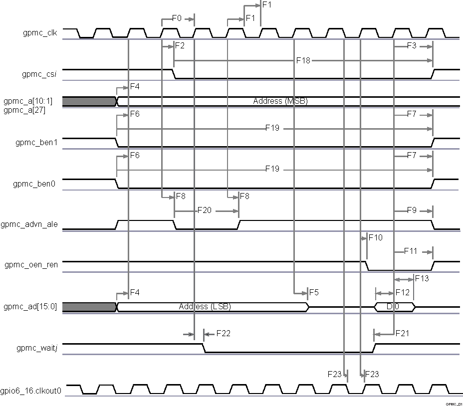 Figure 5-22 GPMC / Multiplexed 16bits NOR Flash - Synchronous Single Read -
(GpmcFCLKDivider = 0)(1)(2)
- In gpmc_csi, i = 0 to 7.
- In gpmc_waitj, j = 0 to 1.
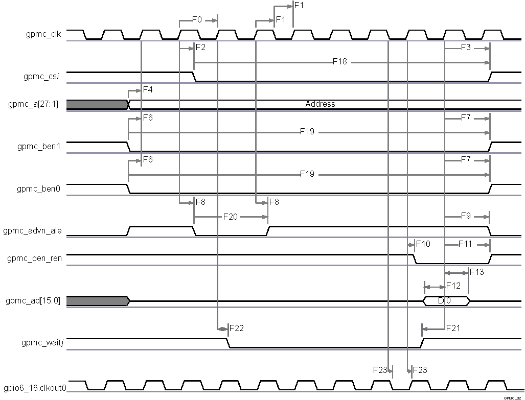 Figure 5-23 GPMC / Non-Multiplexed 16bits NOR Flash - Synchronous Single Read -
(GpmcFCLKDivider = 0)(1)(2)
- In gpmc_csi, i = 0 to 7.
- In gpmc_waitj, j = 0 to 1.
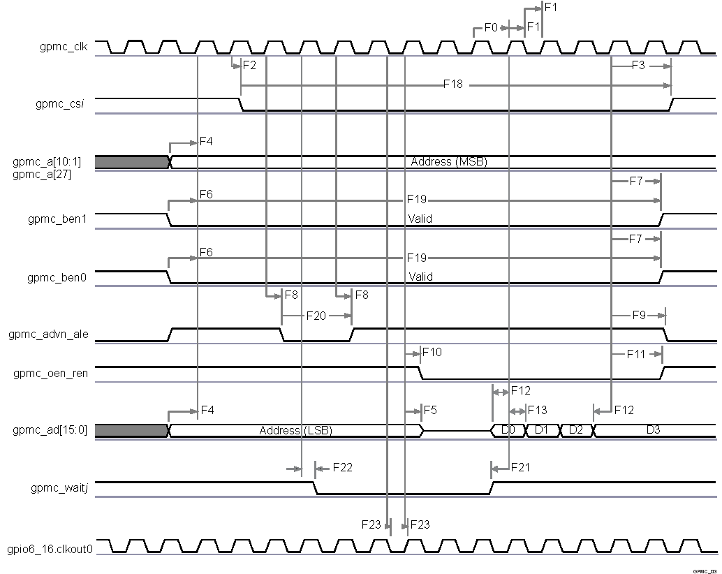 Figure 5-24 GPMC / Multiplexed 16bits NOR Flash - Synchronous Burst Read 4x16 bits -
(GpmcFCLKDivider = 0)(1)(2)
- In gpmc_csi, i= 0 to 7.
- In gpmc_waitj, j = 0 to 1.
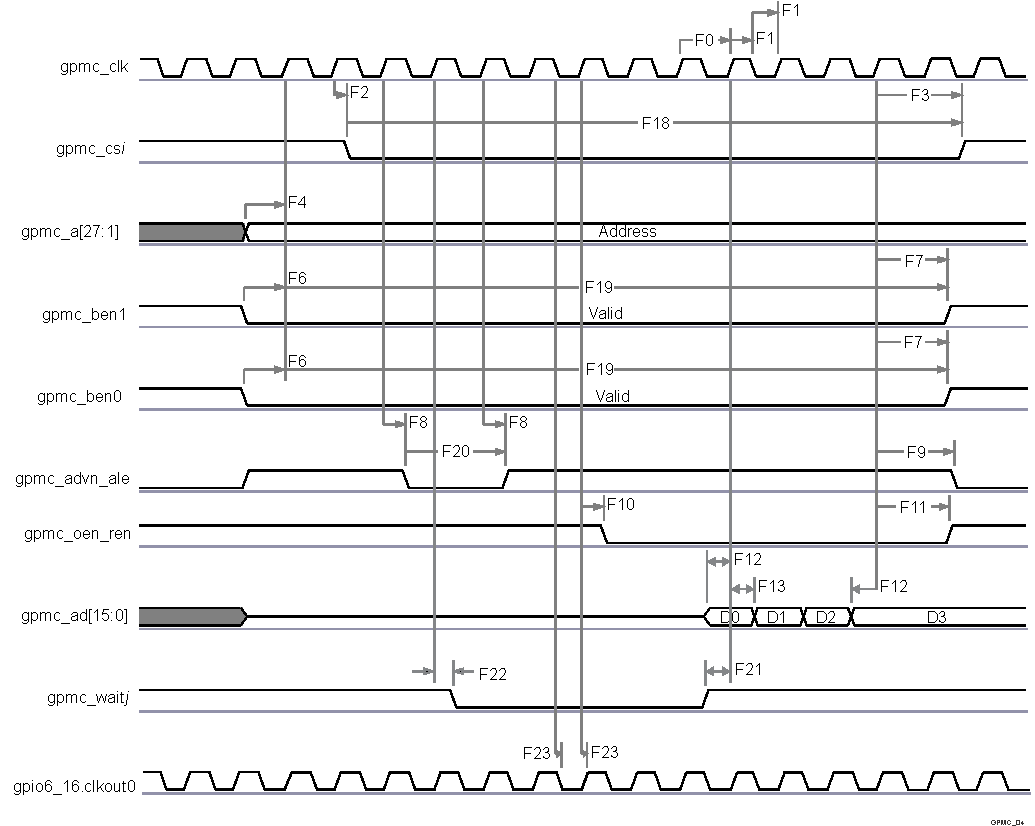 Figure 5-25 GPMC / Non-Multiplexed 16bits NOR Flash - Synchronous Burst Read 4x16 bits -
(GpmcFCLKDivider = 0)(1)(2)
- In gpmc_csi, i = 0 to 7.
- In gpmc_waitj, j = 0 to 1.
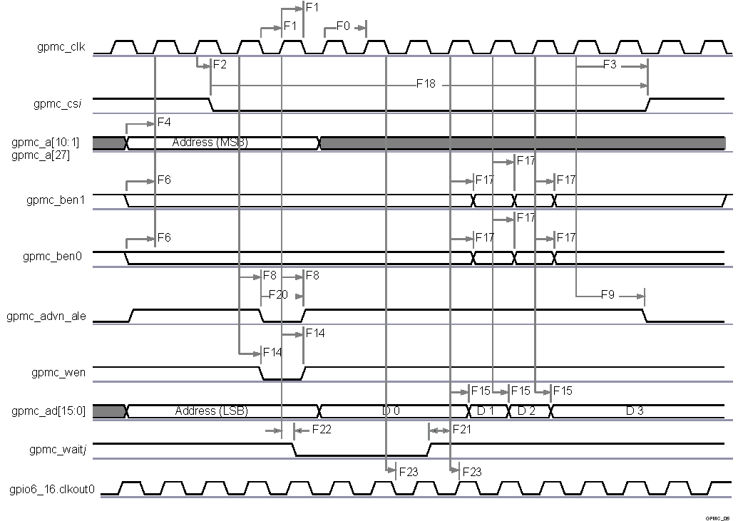 Figure 5-26 GPMC / Multiplexed 16bits NOR Flash - Synchronous Burst Write 4x16bits -
(GpmcFCLKDivider = 0)(1)(2)
- In “gpmc_csi”, i = 0 to 7.
- In “gpmc_waitj”, j = 0 to 1.
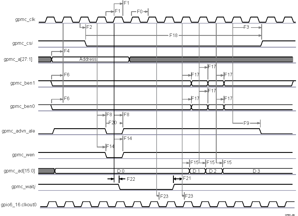 Figure 5-27 GPMC / Non-Multiplexed 16bits NOR Flash - Synchronous Burst Write 4x16bits - (GpmcFCLKDivider = 0)(1)(2)
 - In “gpmc_csi”, i = 1 to 7.
- In “gpmc_waitj”, j = 0 to 1.