SLAS955A March 2013 – July 2015 DRV10963
PRODUCTION DATA.
- 1 Features
- 2 Applications
- 3 Description
- 4 Revision History
- 5 Pin Configuration and Functions
- 6 Specifications
-
7 Detailed Description
- 7.1 Overview
- 7.2 Functional Block Diagram
- 7.3
Feature Description
- 7.3.1 Speed Input and Control
- 7.3.2 Spin up Settings
- 7.3.3 Motor Direction Change
- 7.3.4 Motor Frequency Feedback (FG)
- 7.3.5 Lock Detection
- 7.3.6 Soft Current Limit
- 7.3.7 Short Circuit Current Protection
- 7.3.8 Anti-Voltage Surge (AVS)
- 7.3.9 Control Advance Angle
- 7.3.10 Overtemperature Protection
- 7.3.11 Undervoltage Protection
- 7.3.12 OTP Configuration
- 7.4 Device Functional Modes
- 8 Application and Implementation
- 9 Power Supply Recommendations
- 10Layout
- 11Device and Documentation Support
- 12Mechanical, Packaging, and Orderable Information
パッケージ・オプション
メカニカル・データ(パッケージ|ピン)
- DSN|10
サーマルパッド・メカニカル・データ
- DSN|10
発注情報
8 Application and Implementation
NOTE
Information in the following applications sections is not part of the TI component specification, and TI does not warrant its accuracy or completeness. TI’s customers are responsible for determining suitability of components for their purposes. Customers should validate and test their design implementation to confirm system functionality.
8.1 Application Information
DRV10963 is used in sensorless 3-phase BLDC motor control. The driver provides a high performance, high reliability, flexible and simple solution for compute fan applications. The following design shows a common application of the DRV10963.
8.2 Typical Application
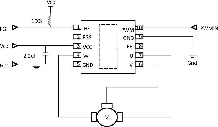
 Figure 17. Typical Application Schematic
8.2.1 Design Requirements
Table 11 lists several key motor characteristics and recommended ranges which the DRV10963 is capable of driving. However, that does not necessarily mean motors outside these boundaries cannot be driven by DRV10963.
Recommended ranges listed in Table 11 can serve as a general guideline to quickly decide whether DRV10963 is a good fit for an application. Motor performance is not ensured for all uses.
Table 11. Key Motor Characteristics and Recommended Ranges
| Rm (Ω) | Lm (µH) | Kt (mV/Hz) | fFG_max (Hz) | |
|---|---|---|---|---|
| Recommended Value | 2.5 ~ 36 | 50 ~ 10000 | 1 ~ 100 | 1300 |
Rm - Motor phase resistance between phase to phase;
Lm - Motor phase to phase inductance between phase to phase;
Kt - Motor BEMF constant from phase to center tape;
fFG_max - Maximum electrical frequency. Maximum motor speed can be calculated from:
- If FGS = 1, RPM = (fFG_max × 60)/ number of pole pairs
- If FGS = 0, RPM = (fFG_max × 120)/ number of pole pairs
8.2.2 Detailed Design Procedure
1. Refer to Design Requirements and make sure your system meets the recommended application range.
2. Refer to the DRV10963 Tuning Guide and measure the motor parameters.
3. Refer to the DRV10963 Tuning Guide. Configure the parameters using DRV10963 GUI, and optimize the motor operation. The Tuning Guide takes the user through all the configurations step by step, including: start-up operation, closed-loop operation, current control, initial positioning, lock detection, and anti-voltage surge.
4. Build your hardware based on Layout Guidelines.
5. Connect the device into system and validate your system solution
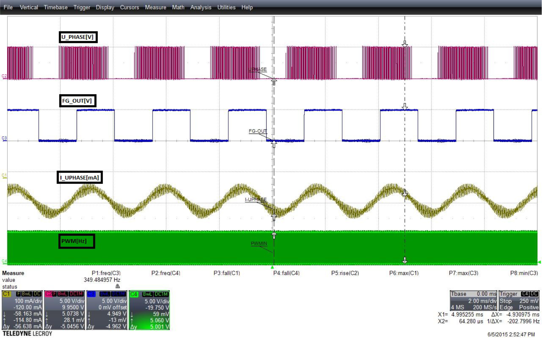
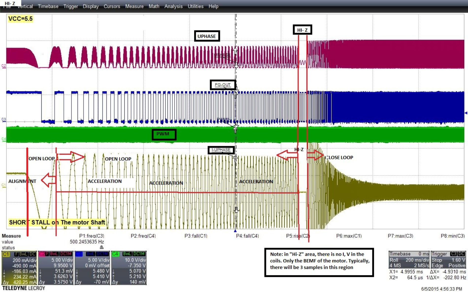
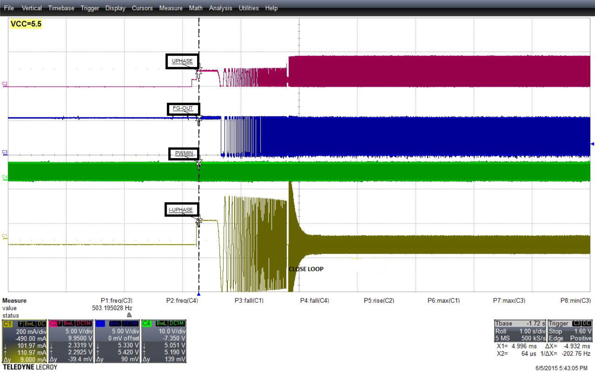
8.2.3 Application Curves


