JAJSEE8G July   2014  – February 2018 DRV10983

PRODUCTION DATA.  

  1. 特長
  2. アプリケーション
  3. 概要
    1.     Device Images
      1.      アプリケーションの回路図
  4. 改訂履歴
  5. 概要(続き)
  6. Pin Configuration and Functions
    1.     Pin Functions
  7. Specifications
    1. 7.1 Absolute Maximum Ratings
    2. 7.2 ESD Ratings
    3. 7.3 Recommended Operating Conditions
    4. 7.4 Thermal Information
    5. 7.5 Electrical Characteristics
    6. 7.6 Typical Characteristics
  8. Detailed Description
    1. 8.1 Overview
    2. 8.2 Functional Block Diagram
    3. 8.3 Feature Description
      1. 8.3.1 Regulators
        1. 8.3.1.1 Step-Down Regulator
        2. 8.3.1.2 3.3-V and 1.8-V LDO
      2. 8.3.2 Protection Circuits
        1. 8.3.2.1 Thermal Shutdown
        2. 8.3.2.2 Undervoltage Lockout (UVLO)
        3. 8.3.2.3 Overcurrent Protection (OCP)
        4. 8.3.2.4 Lock
      3. 8.3.3 Motor Speed Control
      4. 8.3.4 Sleep or Standby Condition
      5. 8.3.5 Non-Volatile Memory
    4. 8.4 Device Functional Modes
      1. 8.4.1  Motor Parameters
        1. 8.4.1.1 Motor Phase Resistance
        2. 8.4.1.2 BEMF Constant
      2. 8.4.2  Starting the Motor Under Different Initial Conditions
        1. 8.4.2.1 Case 1 – Motor Is Stationary
        2. 8.4.2.2 Case 2 – Motor Is Spinning in the Forward Direction
        3. 8.4.2.3 Case 3 – Motor Is Spinning in the Reverse Direction
      3. 8.4.3  Motor Start Sequence
        1. 8.4.3.1 ISD
        2. 8.4.3.2 Motor Resynchronization
        3. 8.4.3.3 Reverse Drive
        4. 8.4.3.4 Motor Brake
        5. 8.4.3.5 Motor Initialization
          1. 8.4.3.5.1 Align
          2. 8.4.3.5.2 Initial Position Detect (IPD)
            1. 8.4.3.5.2.1 IPD Operation
            2. 8.4.3.5.2.2 IPD Release Mode
            3. 8.4.3.5.2.3 IPD Advance Angle
          3. 8.4.3.5.3 Motor Start
        6. 8.4.3.6 Start-Up Timing
      4. 8.4.4  Start-Up Current Setting
        1. 8.4.4.1 Start-Up Current Ramp-Up
      5. 8.4.5  Closed Loop
        1. 8.4.5.1 Half Cycle Control and Full Cycle Control
        2. 8.4.5.2 Analog Mode Speed Control
        3. 8.4.5.3 Digital PWM Input Mode Speed Control
        4. 8.4.5.4 I2C Mode Speed Control
        5. 8.4.5.5 Closed Loop Accelerate
        6. 8.4.5.6 Control Coefficient
        7. 8.4.5.7 Commutation Control Advance Angle
      6. 8.4.6  Current Limit
        1. 8.4.6.1 Acceleration Current Limit
      7. 8.4.7  Lock Detect and Fault Handling
        1. 8.4.7.1 Lock0: Lock Detection Current Limit Triggered
        2. 8.4.7.2 Lock1: Abnormal Speed
        3. 8.4.7.3 Lock2: Abnormal Kt
        4. 8.4.7.4 Lock3 (Fault3): No Motor Fault
        5. 8.4.7.5 Lock4: Open Loop Motor Stuck Lock
        6. 8.4.7.6 Lock5: Closed Loop Motor Stuck Lock
      8. 8.4.8  AVS Function
        1. 8.4.8.1 Mechanical AVS Function
      9. 8.4.9  PWM Output
      10. 8.4.10 FG Customized Configuration
        1. 8.4.10.1 FG Output Frequency
        2. 8.4.10.2 FG Open-Loop and Lock Behavior
      11. 8.4.11 Diagnostics and Visibility
        1. 8.4.11.1 Motor Status Readback
        2. 8.4.11.2 Motor Speed Readback
          1. 8.4.11.2.1 Two-Byte Register Readback
        3. 8.4.11.3 Motor Electrical Period Readback
        4. 8.4.11.4 BEMF Constant Readback
        5. 8.4.11.5 Motor Estimated Position by IPD
        6. 8.4.11.6 Supply Voltage Readback
        7. 8.4.11.7 Speed Command Readback
        8. 8.4.11.8 Speed Command Buffer Readback
        9. 8.4.11.9 Fault Diagnostics
    5. 8.5 Register Maps
      1. 8.5.1 I2C Serial Interface
      2. 8.5.2 Register Map
      3. 8.5.3 Register Definition
        1. Table 9. Register Description
  9. Application and Implementation
    1. 9.1 Application Information
    2. 9.2 Typical Application
      1. 9.2.1 Design Requirements
      2. 9.2.2 Detailed Design Procedure
      3. 9.2.3 Application Curves
  10. 10Power Supply Recommendations
  11. 11Layout
    1. 11.1 Layout Guidelines
    2. 11.2 Layout Example
  12. 12デバイスおよびドキュメントのサポート
    1. 12.1 デバイス・サポート
      1. 12.1.1 デベロッパー・ネットワークの製品に関する免責事項
    2. 12.2 ドキュメントのサポート
      1. 12.2.1 関連資料
    3. 12.3 商標
    4. 12.4 静電気放電に関する注意事項
    5. 12.5 ドキュメントの更新通知を受け取る方法
    6. 12.6 コミュニティ・リソース
    7. 12.7 Glossary
  13. 13メカニカル、パッケージ、および注文情報

パッケージ・オプション

メカニカル・データ(パッケージ|ピン)
サーマルパッド・メカニカル・データ
発注情報

Lock Detect and Fault Handling

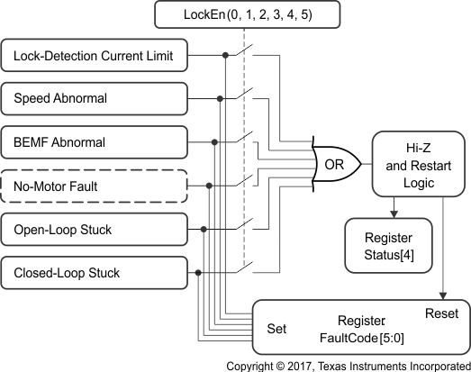
The DRV10983 provides several options for determining if the motor becomes locked as a result of some external torque. Five lock detect schemes work together to ensure the lock condition is detected quickly and reliably. Figure 29 shows the logic which integrates the various lock detect schemes. When a lock condition is detected, the DRV10983 device takes action to prevent continuously driving the motor in order to prevent damage to the system or the motor.

In addition to detecting if there is a locked motor condition, the DRV10983 also identifies and takes action if there is no motor connected to the system.

Each of the five lock-detect schemes and the no motor detection can be disabled by respective register bits LockEn[5:0].

When a lock condition is detected, the MtrLck in the Status register is set. The FaultCode register provides an indication of which of the six different conditions was detected on Lock5 to Lock0. These bits are reset when the motor restarts. The bits in the FaultCode register are set even if the lock detect scheme is disabled.

The DRV10983 reacts to either locked rotor or no motor connected conditions by putting the output drivers into a high-impedance state. To prevent the energy in the motor from pumping the supply voltage, the DRV10983 incorporates an anti-voltage-surge (AVS) process whenever the output stages transition into the high-impedance state. The AVS function is described in AVS Function. After entering the high-impedance state as a result of a fault condition, the system tries to restart after tLOCK_OFF.
DRV10983 DRV10983Z lock_det_fault_diag_LVSCP6.gifFigure 29. Lock Detect and Fault Diagnose