JAJSEE8G July   2014  – February 2018 DRV10983

PRODUCTION DATA.  

  1. 特長
  2. アプリケーション
  3. 概要
    1.     Device Images
      1.      アプリケーションの回路図
  4. 改訂履歴
  5. 概要(続き)
  6. Pin Configuration and Functions
    1.     Pin Functions
  7. Specifications
    1. 7.1 Absolute Maximum Ratings
    2. 7.2 ESD Ratings
    3. 7.3 Recommended Operating Conditions
    4. 7.4 Thermal Information
    5. 7.5 Electrical Characteristics
    6. 7.6 Typical Characteristics
  8. Detailed Description
    1. 8.1 Overview
    2. 8.2 Functional Block Diagram
    3. 8.3 Feature Description
      1. 8.3.1 Regulators
        1. 8.3.1.1 Step-Down Regulator
        2. 8.3.1.2 3.3-V and 1.8-V LDO
      2. 8.3.2 Protection Circuits
        1. 8.3.2.1 Thermal Shutdown
        2. 8.3.2.2 Undervoltage Lockout (UVLO)
        3. 8.3.2.3 Overcurrent Protection (OCP)
        4. 8.3.2.4 Lock
      3. 8.3.3 Motor Speed Control
      4. 8.3.4 Sleep or Standby Condition
      5. 8.3.5 Non-Volatile Memory
    4. 8.4 Device Functional Modes
      1. 8.4.1  Motor Parameters
        1. 8.4.1.1 Motor Phase Resistance
        2. 8.4.1.2 BEMF Constant
      2. 8.4.2  Starting the Motor Under Different Initial Conditions
        1. 8.4.2.1 Case 1 – Motor Is Stationary
        2. 8.4.2.2 Case 2 – Motor Is Spinning in the Forward Direction
        3. 8.4.2.3 Case 3 – Motor Is Spinning in the Reverse Direction
      3. 8.4.3  Motor Start Sequence
        1. 8.4.3.1 ISD
        2. 8.4.3.2 Motor Resynchronization
        3. 8.4.3.3 Reverse Drive
        4. 8.4.3.4 Motor Brake
        5. 8.4.3.5 Motor Initialization
          1. 8.4.3.5.1 Align
          2. 8.4.3.5.2 Initial Position Detect (IPD)
            1. 8.4.3.5.2.1 IPD Operation
            2. 8.4.3.5.2.2 IPD Release Mode
            3. 8.4.3.5.2.3 IPD Advance Angle
          3. 8.4.3.5.3 Motor Start
        6. 8.4.3.6 Start-Up Timing
      4. 8.4.4  Start-Up Current Setting
        1. 8.4.4.1 Start-Up Current Ramp-Up
      5. 8.4.5  Closed Loop
        1. 8.4.5.1 Half Cycle Control and Full Cycle Control
        2. 8.4.5.2 Analog Mode Speed Control
        3. 8.4.5.3 Digital PWM Input Mode Speed Control
        4. 8.4.5.4 I2C Mode Speed Control
        5. 8.4.5.5 Closed Loop Accelerate
        6. 8.4.5.6 Control Coefficient
        7. 8.4.5.7 Commutation Control Advance Angle
      6. 8.4.6  Current Limit
        1. 8.4.6.1 Acceleration Current Limit
      7. 8.4.7  Lock Detect and Fault Handling
        1. 8.4.7.1 Lock0: Lock Detection Current Limit Triggered
        2. 8.4.7.2 Lock1: Abnormal Speed
        3. 8.4.7.3 Lock2: Abnormal Kt
        4. 8.4.7.4 Lock3 (Fault3): No Motor Fault
        5. 8.4.7.5 Lock4: Open Loop Motor Stuck Lock
        6. 8.4.7.6 Lock5: Closed Loop Motor Stuck Lock
      8. 8.4.8  AVS Function
        1. 8.4.8.1 Mechanical AVS Function
      9. 8.4.9  PWM Output
      10. 8.4.10 FG Customized Configuration
        1. 8.4.10.1 FG Output Frequency
        2. 8.4.10.2 FG Open-Loop and Lock Behavior
      11. 8.4.11 Diagnostics and Visibility
        1. 8.4.11.1 Motor Status Readback
        2. 8.4.11.2 Motor Speed Readback
          1. 8.4.11.2.1 Two-Byte Register Readback
        3. 8.4.11.3 Motor Electrical Period Readback
        4. 8.4.11.4 BEMF Constant Readback
        5. 8.4.11.5 Motor Estimated Position by IPD
        6. 8.4.11.6 Supply Voltage Readback
        7. 8.4.11.7 Speed Command Readback
        8. 8.4.11.8 Speed Command Buffer Readback
        9. 8.4.11.9 Fault Diagnostics
    5. 8.5 Register Maps
      1. 8.5.1 I2C Serial Interface
      2. 8.5.2 Register Map
      3. 8.5.3 Register Definition
        1. Table 9. Register Description
  9. Application and Implementation
    1. 9.1 Application Information
    2. 9.2 Typical Application
      1. 9.2.1 Design Requirements
      2. 9.2.2 Detailed Design Procedure
      3. 9.2.3 Application Curves
  10. 10Power Supply Recommendations
  11. 11Layout
    1. 11.1 Layout Guidelines
    2. 11.2 Layout Example
  12. 12デバイスおよびドキュメントのサポート
    1. 12.1 デバイス・サポート
      1. 12.1.1 デベロッパー・ネットワークの製品に関する免責事項
    2. 12.2 ドキュメントのサポート
      1. 12.2.1 関連資料
    3. 12.3 商標
    4. 12.4 静電気放電に関する注意事項
    5. 12.5 ドキュメントの更新通知を受け取る方法
    6. 12.6 コミュニティ・リソース
    7. 12.7 Glossary
  13. 13メカニカル、パッケージ、および注文情報

パッケージ・オプション

メカニカル・データ(パッケージ|ピン)
サーマルパッド・メカニカル・データ
発注情報

FG Open-Loop and Lock Behavior

Note that the FG output reflects the driving state of the motor. During normal closed loop behavior, the driving state and the actual state of the motor are synchronized. During open loop acceleration, however, this may not reflect the actual motor speed. During a locked motor condition, the FG output is driven high.

The DRV10983 provides three options for controlling the FG output during open loop as shown in Figure 37. The selection of these options is determined by the FGOLsel[1:0] setting.

  • Option0: Open loop output FG based on driving frequency
  • Option1: Open loop no FG output (keep high)
  • Option2: FG output based on driving frequency at the first power-on start-up, and no FG output (keep high) for any subsequent restarts
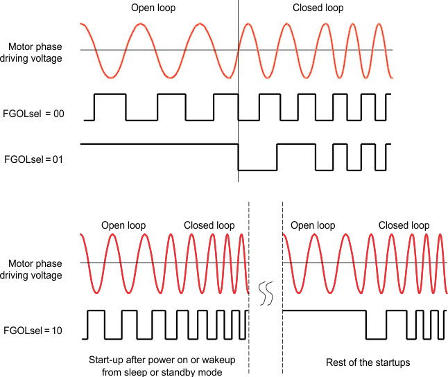
DRV10983 DRV10983Z FB_behav_open2_LVSCP2.gifFigure 37. FG Behavior During Open Loop