JAJSF37D May   2014  – March 2018 DRV2605L

PRODUCTION DATA.  

  1. 特長
  2. アプリケーション
  3. 概要
    1.     概略回路図
  4. 改訂履歴
  5. 概要(続き)
  6. Pin Configuration and Functions
    1.     Pin Functions
    2.     Pin Functions
  7. Specifications
    1. 7.1 Absolute Maximum Ratings
    2. 7.2 ESD Ratings
    3. 7.3 Recommended Operating Conditions
    4. 7.4 Thermal Information
    5. 7.5 Electrical Characteristics
    6. 7.6 Timing Requirements
    7. 7.7 Switching Characteristics
    8. 7.8 Typical Characteristics
  8. Parameter Measurement Information
    1. 8.1 Test Setup for Graphs
      1. 8.1.1 Default Test Conditions
  9. Detailed Description
    1. 9.1 Overview
    2. 9.2 Functional Block Diagram
    3. 9.3 Feature Description
      1. 9.3.1  Support for ERM and LRA Actuators
      2. 9.3.2  Smart-Loop Architecture
        1. 9.3.2.1 Auto-Resonance Engine for LRA
        2. 9.3.2.2 Real-Time Resonance-Frequency Reporting for LRA
        3. 9.3.2.3 Automatic Switch to Open-Loop for LRA
        4. 9.3.2.4 Automatic Overdrive and Braking
          1. 9.3.2.4.1 Startup Boost
          2. 9.3.2.4.2 Brake Factor
          3. 9.3.2.4.3 Brake Stabilizer
        5. 9.3.2.5 Automatic Level Calibration
          1. 9.3.2.5.1 Automatic Compensation for Resistive Losses
          2. 9.3.2.5.2 Automatic Back-EMF Normalization
          3. 9.3.2.5.3 Calibration Time Adjustment
          4. 9.3.2.5.4 Loop-Gain Control
          5. 9.3.2.5.5 Back-EMF Gain Control
        6. 9.3.2.6 Actuator Diagnostics
        7. 9.3.2.7 Automatic Re-Synchronization
      3. 9.3.3  Open-Loop Operation for LRA
      4. 9.3.4  Open-Loop Operation for ERM
      5. 9.3.5  Flexible Front-End Interface
        1. 9.3.5.1 PWM Interface
        2. 9.3.5.2 Internal Memory Interface
          1. 9.3.5.2.1 Waveform Sequencer
          2. 9.3.5.2.2 Library Parameterization
        3. 9.3.5.3 Real-Time Playback (RTP) Interface
        4. 9.3.5.4 Analog Input Interface
        5. 9.3.5.5 Audio-to-Vibe Interface
        6. 9.3.5.6 Input Trigger Option
          1. 9.3.5.6.1 I2C Trigger
          2. 9.3.5.6.2 Edge Trigger
          3. 9.3.5.6.3 Level Trigger
        7. 9.3.5.7 Noise Gate Control
      6. 9.3.6  Edge Rate Control
      7. 9.3.7  Constant Vibration Strength
      8. 9.3.8  Battery Voltage Reporting
      9. 9.3.9  One-Time Programmable (OTP) Memory for Configuration
      10. 9.3.10 Low-Power Standby
      11. 9.3.11 I2C Watchdog Timer
      12. 9.3.12 Device Protection
        1. 9.3.12.1 Thermal Protection
        2. 9.3.12.2 Overcurrent Protection of the Actuator
        3. 9.3.12.3 Overcurrent Protection of the Regulator
        4. 9.3.12.4 Brownout Protection
    4. 9.4 Device Functional Modes
      1. 9.4.1 Power States
        1. 9.4.1.1 Operation With VDD < 2 V (Minimum VDD)
        2. 9.4.1.2 Operation With VDD > 5.5 V (Absolute Maximum VDD)
        3. 9.4.1.3 Operation With EN Control
        4. 9.4.1.4 Operation With STANDBY Control
        5. 9.4.1.5 Operation With DEV_RESET Control
        6. 9.4.1.6 Operation in the Active State
      2. 9.4.2 Changing Modes of Operation
      3. 9.4.3 Operation of the GO Bit
      4. 9.4.4 Operation During Exceptional Conditions
        1. 9.4.4.1 Operation With No Actuator Attached
        2. 9.4.4.2 Operation With a Non-Moving Actuator Attached
        3. 9.4.4.3 Operation With a Short at REG Pin
        4. 9.4.4.4 Operation With a Short at OUT+, OUT–, or Both
    5. 9.5 Programming
      1. 9.5.1 Auto-Resonance Engine Programming for the LRA
        1. 9.5.1.1 Drive-Time Programming
        2. 9.5.1.2 Current-Dissipation Time Programming
        3. 9.5.1.3 Blanking Time Programming
        4. 9.5.1.4 Zero-Crossing Detect-Time Programming
      2. 9.5.2 Automatic-Level Calibration Programming
        1. 9.5.2.1 Rated Voltage Programming
        2. 9.5.2.2 Overdrive Voltage-Clamp Programming
      3. 9.5.3 I2C Interface
        1. 9.5.3.1 General I2C Operation
        2. 9.5.3.2 Single-Byte and Multiple-Byte Transfers
        3. 9.5.3.3 Single-Byte Write
        4. 9.5.3.4 Multiple-Byte Write and Incremental Multiple-Byte Write
        5. 9.5.3.5 Single-Byte Read
        6. 9.5.3.6 Multiple-Byte Read
      4. 9.5.4 Programming for Open-Loop Operation
        1. 9.5.4.1 Programming for ERM Open-Loop Operation
        2. 9.5.4.2 Programming for LRA Open-Loop Operation
      5. 9.5.5 Programming for Closed-Loop Operation
      6. 9.5.6 Auto Calibration Procedure
      7. 9.5.7 Programming On-Chip OTP Memory
      8. 9.5.8 Waveform Playback Programming
        1. 9.5.8.1 Data Formats for Waveform Playback
          1. 9.5.8.1.1 Open-Loop Mode
          2. 9.5.8.1.2 Closed-Loop Mode, Unidirectional
          3. 9.5.8.1.3 Closed-Loop Mode, Bidirectional
        2. 9.5.8.2 Waveform Setup and Playback
          1. 9.5.8.2.1 Waveform Playback Using RTP Mode
          2. 9.5.8.2.2 Waveform Playback Using the Analog-Input Mode
          3. 9.5.8.2.3 Waveform Playback Using PWM Mode
          4. 9.5.8.2.4 Waveform Playback Using Audio-to-Vibe Mode
          5. 9.5.8.2.5 Waveform Sequencer
          6. 9.5.8.2.6 Waveform Triggers
    6. 9.6 Register Map
      1. 9.6.1  Status (Address: 0x00)
        1. Table 4. Status Register Field Descriptions
      2. 9.6.2  Mode (Address: 0x01)
        1. Table 5. Mode Register Field Descriptions
      3. 9.6.3  Real-Time Playback Input (Address: 0x02)
        1. Table 6. Real-Time Playback Input Register Field Descriptions
      4. 9.6.4  Library Selection (Address: 0x03)
        1. Table 7. Library Selection Register Field Descriptions
      5. 9.6.5  Waveform Sequencer (Address: 0x04 to 0x0B)
        1. Table 8. Waveform Sequencer Register Field Descriptions
      6. 9.6.6  GO (Address: 0x0C)
        1. Table 9. GO Register Field Descriptions
      7. 9.6.7  Overdrive Time Offset (Address: 0x0D)
        1. Table 10. Overdrive Time Offset Register Field Descriptions
      8. 9.6.8  Sustain Time Offset, Positive (Address: 0x0E)
        1. Table 11. Sustain Time Offset, Positive Register Field Descriptions
      9. 9.6.9  Sustain Time Offset, Negative (Address: 0x0F)
        1. Table 12. Sustain Time Offset, Negative Register Field Descriptions
      10. 9.6.10 Brake Time Offset (Address: 0x10)
        1. Table 13. Brake Time Offset Register Field Descriptions
      11. 9.6.11 Audio-to-Vibe Control (Address: 0x11)
        1. Table 14. Audio-to-Vibe Control Register Field Descriptions
      12. 9.6.12 Audio-to-Vibe Minimum Input Level (Address: 0x12)
        1. Table 15. Audio-to-Vibe Minimum Input Level Register Field Descriptions
      13. 9.6.13 Audio-to-Vibe Maximum Input Level (Address: 0x13)
        1. Table 16. Audio-to-Vibe Maximum Input Level Register Field Descriptions
      14. 9.6.14 Audio-to-Vibe Minimum Output Drive (Address: 0x14)
        1. Table 17. Audio-to-Vibe Minimum Output Drive Register Field Descriptions
      15. 9.6.15 Audio-to-Vibe Maximum Output Drive (Address: 0x15)
        1. Table 18. Audio-to-Vibe Maximum Output Drive Register Field Descriptions
      16. 9.6.16 Rated Voltage (Address: 0x16)
        1. Table 19. Rated Voltage Register Field Descriptions
      17. 9.6.17 Overdrive Clamp Voltage (Address: 0x17)
        1. Table 20. Overdrive Clamp Voltage Register Field Descriptions
      18. 9.6.18 Auto-Calibration Compensation Result (Address: 0x18)
        1. Table 21. Auto-Calibration Compensation-Result Register Field Descriptions
      19. 9.6.19 Auto-Calibration Back-EMF Result (Address: 0x19)
        1. Table 22. Auto-Calibration Back-EMF Result Register Field Descriptions
      20. 9.6.20 Feedback Control (Address: 0x1A)
        1. Table 23. Feedback Control Register Field Descriptions
      21. 9.6.21 Control1 (Address: 0x1B)
        1. Table 24. Control1 Register Field Descriptions
      22. 9.6.22 Control2 (Address: 0x1C)
        1. Table 25. Control2 Register Field Descriptions
      23. 9.6.23 Control3 (Address: 0x1D)
        1. Table 26. Control3 Register Field Descriptions
      24. 9.6.24 Control4 (Address: 0x1E)
        1. Table 27. Control4 Register Field Descriptions
      25. 9.6.25 Control5 (Address: 0x1F)
        1. Table 28. Control5 Register Field Descriptions
      26. 9.6.26 LRA Open Loop Period (Address: 0x20)
        1. Table 29. LRA Open Loop Period Register Field Descriptions
      27. 9.6.27 V(BAT) Voltage Monitor (Address: 0x21)
        1. Table 30. V(BAT) Voltage-Monitor Register Field Descriptions
      28. 9.6.28 LRA Resonance Period (Address: 0x22)
        1. Table 31. LRA Resonance-Period Register Field Descriptions
  10. 10Application and Implementation
    1. 10.1 Application Information
    2. 10.2 Typical Application
      1. 10.2.1 Design Requirements
      2. 10.2.2 Detailed Design Procedure
        1. 10.2.2.1 Actuator Selection
          1. 10.2.2.1.1 Eccentric Rotating-Mass Motors (ERM)
          2. 10.2.2.1.2 Linear Resonance Actuators (LRA)
            1. 10.2.2.1.2.1 Auto-Resonance Engine for LRA
        2. 10.2.2.2 Capacitor Selection
        3. 10.2.2.3 Interface Selection
        4. 10.2.2.4 Power Supply Selection
      3. 10.2.3 Application Curves
    3. 10.3 Initialization Setup
      1. 10.3.1 Initialization Procedure
      2. 10.3.2 Typical Usage Examples
        1. 10.3.2.1 Play a Waveform or Waveform Sequence from the ROM Waveform Memory
        2. 10.3.2.2 Play a Real-Time Playback (RTP) Waveform
        3. 10.3.2.3 Play a PWM or Analog Input Waveform
  11. 11Power Supply Recommendations
  12. 12Layout
    1. 12.1 Layout Guidelines
      1. 12.1.1 Trace Width
    2. 12.2 Layout Example
  13. 13デバイスおよびドキュメントのサポート
    1. 13.1 デバイス・サポート
      1. 13.1.1 法的告知
      2. 13.1.2 波形ライブラリのエフェクト一覧
    2. 13.2 ドキュメントのサポート
      1. 13.2.1 関連資料
    3. 13.3 ドキュメントの更新通知を受け取る方法
    4. 13.4 コミュニティ・リソース
    5. 13.5 商標
    6. 13.6 静電気放電に関する注意事項
    7. 13.7 Glossary
  14. 14メカニカル、パッケージ、および注文情報

パッケージ・オプション

メカニカル・データ(パッケージ|ピン)
サーマルパッド・メカニカル・データ
発注情報

Auto Calibration Procedure

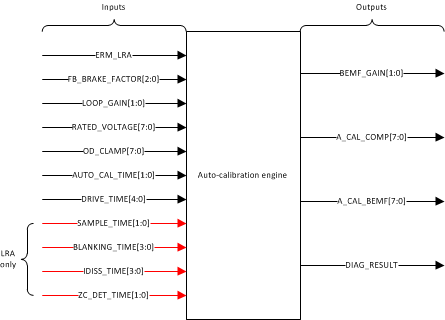
The calibration engine requires a number of bits as inputs before the engine can be executed (see Figure 25). When the inputs are configured, the calibration routine can be executed. After calibration execution occurs, the output parameters are written over the specified register locations. Figure 25 shows all of the required inputs and generated outputs. To ensure proper auto-resonance operation, the LRA actuator type requires more input parameters than the ERM. The LRA parameters are ignored when the device is in ERM mode.

DRV2605L autocalFuncDiag_slos866.gifFigure 25. Calibration-Engine Functional Diagram

Variation occurs between different actuators even if the actuators are of the same model. To ensure optimal results, TI recommends that the calibration routine be run at least once for each actuator. The OTP feature of the DRV2605L device can store the calibration values. Because of the stored values, the calibration procedure does not have run every time. Having a single set of calibration register values that can be loaded during the system initialization is possible.

The following instructions list the step-by-step register configuration for auto-calibration. For additional details see the Register Map section.

  1. Apply the supply voltage to the DRV2605L device, and pull the EN pin high. The supply voltage should allow for adequate drive voltage of the selected actuator.
  2. Write a value of 0x07 to register 0x01. This value moves the DRV2605L device out of STANDBY and places the MODE[2:0] bits in auto-calibration mode.
  3. Populate the input parameters required by the auto-calibration engine:
    1. ERM_LRA — selection will depend on desired actuator.
    2. FB_BRAKE_FACTOR[2:0] — A value of 2 is valid for most actuators.
    3. LOOP_GAIN[1:0] — A value of 2 is valid for most actuators.
    4. RATED_VOLTAGE[7:0] — See the Rated Voltage Programming section for calculating the correct register value.
    5. OD_CLAMP[7:0] — See the Overdrive Voltage-Clamp Programming section for calculating the correct register value.
    6. AUTO_CAL_TIME[1:0] — A value of 3 is valid for most actuators.
    7. DRIVE_TIME[3:0] — See the Drive-Time Programming for calculating the correct register value.
    8. SAMPLE_TIME[1:0] — A value of 3 is valid for most actuators.
    9. BLANKING_TIME[3:0] — A value of 1 is valid for most actuators.
    10. IDISS_TIME[3:0] — A value of 1 is valid for most actuators.
    11. ZC_DET_TIME[1:0] — A value of 0 is valid for most actuators.
  4. Set the GO bit (write 0x01 to register 0x0C) to start the auto-calibration process. When auto calibration is complete, the GO bit automatically clears. The auto-calibration results are written in the respective registers as shown in Figure 25.
  5. Check the status of the DIAG_RESULT bit (in register 0x00) to ensure that the auto-calibration routine is complete without faults.
  6. Evaluate system performance with the auto-calibrated settings. Note that the evaluation should occur during the final assembly of the device because the auto-calibration process can affect actuator performance and behavior. If any adjustment is required, the inputs can be modified and this sequence can be repeated. If the performance is satisfactory, the user can do any of the following:
    1. Repeat the calibration process upon subsequent power ups.
    2. Store the auto-calibration results in host processor memory and rewrite them to the DRV2605L device upon subsequent power ups. The device retains these settings when in STANDBY mode or when the EN pin is low.
    3. Program the results permanently in nonvolatile, on-chip OTP memory. Even when a device power cycle occurs, the device retains the auto-calibration settings. See the Programming On-Chip OTP Memory section for additional information.