JAJSGK4E March 2013 – January 2023 DRV2667
PRODUCTION DATA
- 1 特長
- 2 アプリケーション
- 3 概要
- 4 Revision History
- 5 Pin Configuration and Functions
- 6 Specifications
-
7 Detailed Description
- 7.1 Overview
- 7.2 Functional Block Diagram
- 7.3
Feature Description
- 7.3.1 Support for Haptic Piezo Actuators
- 7.3.2 Flexible Front End Interface
- 7.3.3 Ramp Down Behavior
- 7.3.4 Low Latency Startup
- 7.3.5 Low Power Standby Mode
- 7.3.6 Device Reset
- 7.3.7 Amplifier Gain
- 7.3.8 Adjustable Boost Voltage
- 7.3.9 Adjustable Current Limit
- 7.3.10 Internal Charge Pump
- 7.3.11 Device Protection
- 7.4 Device Functional Modes
- 7.5 Programming
- 7.6 Register Map
- 8 Application and Implementation
- 9 Power Supply Recommendations
- 10Layout
- 11Device and Documentation Support
- 12Mechanical, Packaging, and Orderable Information
パッケージ・オプション
メカニカル・データ(パッケージ|ピン)
- RGP|20
サーマルパッド・メカニカル・データ
- RGP|20
発注情報
7.5.3.2 RAM Format
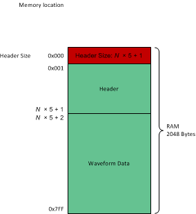
The RAM is structured into 3 main blocks as shown in #SLOS905DESC00P2:
- Header size block; 1 byte
- Header block; N x 5 bytes, where N is the number of effects stored
- Waveform data block
 Figure 7-5 RAM Structure
The first byte of the RAM (at memory location 0x00 on Page 1) must contain the header size. The header size refers to the last byte in the header, so the value stored must be N x 5 + 1, as shown in #SLOS905DESC00P2.
The header block describes the location of the waveform data content. The structure of the header consists of 5-byte blocks containing the following information (see #SLOS905DESC00P3):
- Start address, upper byte
- Start address, lower byte
- Stop address, upper byte
- Stop address, lower byte
- Repeat count
 Figure 7-6 Header Format
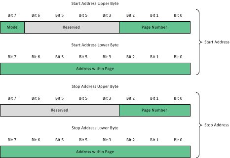
Because more than 8-bits are required to address the 2 kB of memory, each start and stop address consists of two bytes. The start address contains the location of the first byte in the waveform and the stop byte contains the locations of the last byte in the waveform. Within the address byte, the upper byte contains the page address, and the lower byte refers to the specified address within the page (see #SLOS905DESC00P4). The upper byte interprets a 0 as Page 1, and a 7 as Page 8 because the waveform processing engine cannot access the control space in Page 0.
 Figure 7-7 Header Address Byte Format
The repeat count byte contains the number of times this waveform identifier (which starts at the start address and ends at the stop address) is to be repeated when it is called during playback. A 0 in this byte is interpreted as an infinite loop and the waveform is played indefinitely until the GO bit is cleared by the user. Otherwise, the repeat count is simply the number of times that the waveform is repeated.
The waveform data can be interpreted in two ways:
- Direct Playback from RAM mode
- Waveform Synthesis Playback mode
Note that both modes can be stored in the RAM, and the device interprets the waveform data according to the mode specified. To signal the device which mode is desired, the MSB of the start address, upper byte is used (see #SLOS905DESC00P4). A 0 indicates Direct Playback from RAM Mode, and a 1 indicates a Waveform Synthesis Playback Mode.
The Direct Playback from RAM mode requires no special handling: the waveform starts at the start-address location and plays each sub-sequent byte at the Nyquist-rate. The data is stored in twos complement, where 0xFF is interpreted as full-scale, 0x00 is no signal, and 0x80 is negative full-scale. The waveform is played at an 8-kHz data rate.
The Waveform Synthesis Playback Mode stores data in sinusoidal chunks, where each chunk consists of four bytes as shown in #SLOS905DESC00P5:
- Amplitude
- Frequency
- Number of Cycles (Duration)
- Envelope
 Figure 7-8 Waveform Synthesizer Format
The interpretation of each of these four bytes is outlined in Table 7-3.
| BYTE | NAME | DESCRIPTION | |
|---|---|---|---|
| 1 | Amplitude | The amplitude byte refers to the magnitude of the synthesized sinusoid. 0xFF produces a full-scale sinusoid, 0x80 produces a half-scale sinusoid, and 0x00 does not produce any signal. An amplitude of 0x00 can be useful for producing timed waits or delays within the effect. To calculate the absolute peak voltage, use the following equation, where amplitude is a single-byte integer: Peak voltage = amplitude / 255 x full-scale peak voltage | |
| 2 | Frequency | The frequency byte adjusts the frequency of the synthesized sinusoid. The minimum frequency is 7.8125 Hz. A value of zero is not allowed. The sinusoidal frequency is determined with the following equation, where frequency is a single-byte integer: Sinusoid frequency (Hz) = 7.8125 x frequency | |
| 3 | Number of Cycles (Duration) | The number of sinusoidal cycles to be played by the synthesizer. A convenient way to specify the duration of a coherent sinusoid is by inputting the number of cycles. This method ensures that the waveform chunk will always begin and end at zero amplitude, thus avoiding discontinuities. The actual duration in time given by this value may be calculated through the following equation, where # of cycles and frequency are both single-byte integers. Duration (ms) = 1000 x # of cycles / (7.8125 x frequency) | |
| 4 | Envelope | The envelope byte is divided into two nibbles. The upper nibble, bits [7:4], sets the ramp-up rate at the beginning of the synthesized sinusoid, and the lower nibble, bits [3:0], sets the ramp-down rate at the end of the synthesized sinusoid. The user must note that the ramp-up time is included in the duration parameter of the waveform, and the ramp-down time is appended to the duration parameter of the waveform. As such, if a ramp-up time is used, the ramp-up time must be less than the duration time as programmed in byte 3. Also note that the Total Ramp Time is for a ramp to full-scale amplitude (amplitude = 0xFF). Ramps to a fraction of full-scale have the same fraction of the Total Ramp Time. | |
| Nibble Value | Total Ramp Time | ||
| 0 | No Envelope | ||
| 1 | 32 ms | ||
| 2 | 64 ms | ||
| 3 | 96 ms | ||
| 4 | 128 ms | ||
| 5 | 160 ms | ||
| 6 | 192 ms | ||
| 7 | 224 ms | ||
| 8 | 256 ms | ||
| 9 | 512 ms | ||
| 10 | 768 ms | ||
| 11 | 1024 ms | ||
| 12 | 1280 ms | ||
| 13 | 1536 ms | ||
| 14 | 1792 ms | ||
| 15 | 2048 ms | ||