JAJSHW2A August 2019 – April 2020 DRV425-Q1
PRODUCTION DATA.
- 1 特長
- 2 アプリケーション
- 3 概要
- 4 改訂履歴
- 5 概要(続き)
- 6 Pin Configuration and Functions
- 7 Specifications
- 8 Detailed Description
- 9 Application and Implementation
- 10Power Supply Recommendations
- 11Layout
- 12デバイスおよびドキュメントのサポート
- 13メカニカル、パッケージ、および注文情報
8.3.1.4 Magnetic Field Range, Overrange Indicator, and Error Flag
The measurement range of the DRV425-Q1 is determined by the amount of current driven into the compensation coil and the output voltage range of the shunt-sense amplifier. The maximum compensation current is limited by the supply voltage and the series resistance of the compensation coil and the shunt.
The magnetic field range is adjusted with the external shunt resistor. The DRV425 System Parameter Calculator provides the maximum shunt resistor values depending on the supply voltage (VDD) and the selected reference voltage (VREFIN) for various magnetic field ranges.
For proper operation at a maximum field (BMAX), choose a shunt resistor (RSHUNT) using Equation 3:

where
- VDD = minimum supply voltage of the DRV425-Q1 (V).
- VREFIN = common-mode voltage of the shunt-sense amplifier (V).
- BMAX = desired magnetic field range (T).
Alternatively, to adjust the output voltage of the DRV425-Q1 for a desired maximum voltage (VVOUTMAX), use Equation 4:

where
- VVOUTMAX = desired maximum output voltage at VOUT pin (V).
- BMAX = desired magnetic field range (T).
To avoid railing of the compensation coil driver, make sure that Equation 5 is fulfilled:

where
- BMAX = desired magnetic field range (T).
- RCOIL = compensation coil resistance (Ω).
- VDD = minimum supply voltage of the DRV425-Q1 (V).
- VREFIN = selected internal reference voltage value (V).
The DRV425 System Parameter Calculator is designed to assist with selecting the system parameters.
The DRV425-Q1 offers two diagnostic output pins to detect large fields that exceed the measurement range of the sensor: the overrange indicator (OR) and the ERROR flag.
In normal operation, the DRV425-Q1 sensor feedback loop compensates the magnetic field inside the fluxgate to zero. Therefore, a large field inside the fluxgate indicates that the feedback loop is not properly working, and the sensor output is invalid. To detect this condition, the ERROR pin is pulled low if the internal field exceeds 1.6 mT. The ERROR output is suppressed for 4 µs to 6 µs to prevent an undesired reaction to transients or noise. For static and slowly varying ambient fields, the ERROR pin triggers when the ambient field exceeds the sensor measurement range by more than 1.6 mT. For dynamic magnetic fields that exceed the sensor bandwidth as specified in the Specifications section, the feedback loop response is too slow to accurately compensate the internal field to zero. Therefore, high-frequency fields can trigger the ERROR pin, even if the ambient field does not exceed the measurement range by 1.6 mT.
In addition, the active-low overrange pin (OR) indicates railing of the output of the shunt-sense amplifier. The OR output is suppressed for 2.5 µs to 3.5 µs to prevent an undesired reaction to transients or noise. The OR pin trip level refers to the output voltage value of the shunt-sense amplifier, as specified in the Specifications section. Use Equation 3 and Equation 4 to adjust the OR pin behavior to the specific system-level requirements.
Both the ERROR and OR pins are open-drain outputs that require an external pullup resistor. If desired, connect both pins together with a single pullup resistor to provide a single diagnostic flag.
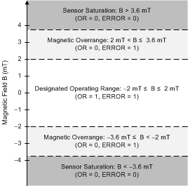
Based on the DRV425 System Parameter Calculator, for a design for a ±2-mT magnetic field input range with a supply of 5 V (±5%), a shunt resistor value of 22 Ω is selected. Figure 63 shows the status of the diagnostic flags in the resulting three operation ranges.
 Figure 63. Magnetic Field Range of the DRV425-Q1 (VDD = 5 V and RSHUNT = 22 Ω)
 With the proper RSHUNT value, the differential amplifier output rails and activates the overrange flag (OR = 0) when the magnetic field exceeds the designated operating range. For fields that exceed the measurement range of the DRV425-Q1 by ≥ 1.6 mT, the fluxgate is saturated and the ERROR pin is pulled low. In this condition, the fluxgate sensor does not provide a valid output value; therefore, the output VOUT of the DRV425-Q1 must be ignored. In applications where the ERROR pin cannot be separately monitored, combine the VOUT and ERROR outputs as shown in Figure 64. This method indicates that a magnetic field is outside of the sensor range by pulling the device output to ground.
 Figure 64. Field Overrange Detection Using a Combined VOUT and ERROR Pin