JAJSHW2A August   2019  – April 2020 DRV425-Q1

PRODUCTION DATA.  

  1. 特長
  2. アプリケーション
  3. 概要
    1.     Device Images
      1.      概略回路図
  4. 改訂履歴
  5. 概要(続き)
  6. Pin Configuration and Functions
    1.     Pin Functions
  7. Specifications
    1. 7.1 Absolute Maximum Ratings
    2. 7.2 ESD Ratings
    3. 7.3 Recommended Operating Conditions
    4. 7.4 Thermal Information
    5. 7.5 Electrical Characteristics
    6. 7.6 Typical Characteristics
  8. Detailed Description
    1. 8.1 Overview
    2. 8.2 Functional Block Diagram
    3. 8.3 Feature Description
      1. 8.3.1 Fluxgate Sensor Front-End
        1. 8.3.1.1 Fluxgate Sensor
        2. 8.3.1.2 Bandwidth
        3. 8.3.1.3 Differential Driver for the Internal Compensation Coil
        4. 8.3.1.4 Magnetic Field Range, Overrange Indicator, and Error Flag
      2. 8.3.2 Shunt-Sense Amplifier
      3. 8.3.3 Voltage Reference
      4. 8.3.4 Low-Power Operation
    4. 8.4 Device Functional Modes
  9. Application and Implementation
    1. 9.1 Application Information
    2. 9.2 Typical Applications
      1. 9.2.1 Linear Position Sensing
        1. 9.2.1.1 Design Requirements
        2. 9.2.1.2 Detailed Design Procedure
        3. 9.2.1.3 Application Curves
      2. 9.2.2 Current Sensing in Busbars
        1. 9.2.2.1 Design Requirements
        2. 9.2.2.2 Detailed Design Procedure
        3. 9.2.2.3 Application Curves
  10. 10Power Supply Recommendations
    1. 10.1 Power Supply Decoupling
    2. 10.2 Power-On Start-Up and Brownout
    3. 10.3 Power Dissipation
      1. 10.3.1 Thermal Pad
  11. 11Layout
    1. 11.1 Layout Guidelines
    2. 11.2 Layout Example
  12. 12デバイスおよびドキュメントのサポート
    1. 12.1 ドキュメントのサポート
      1. 12.1.1 関連資料
    2. 12.2 ドキュメントの更新通知を受け取る方法
    3. 12.3 サポート・リソース
    4. 12.4 商標
    5. 12.5 静電気放電に関する注意事項
    6. 12.6 Glossary
  13. 13メカニカル、パッケージ、および注文情報

パッケージ・オプション

メカニカル・データ(パッケージ|ピン)
サーマルパッド・メカニカル・データ
発注情報

Application Curves

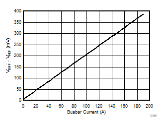
Figure 74 and Figure 75 show the measurement results on a 16-mm wide and 6-mm thick copper busbar with a 12-mm hole diameter using the circuit shown in Figure 73. The two DRV425-Q1 devices are placed at a distance of 1 mm from each other on opposite sides of the PCB. The measurement range is ±500 A; measurement results are limited by test setup. Independent operation of the two DRV425-Q1 sensors increases the measurement range to ±1000 A with the same busbar geometry.
DRV425-Q1 D066_SBOS729.gif
Figure 74. Analog Output Voltage vs
Busbar Current
DRV425-Q1 D067_SBOS729.gif
Figure 75. Linearity Error vs Busbar Current