SBOS729A October 2015 – March 2016 DRV425
PRODUCTION DATA.
- 1 Features
- 2 Applications
- 3 Description
- 4 Revision History
- 5 Pin Configuration and Functions
- 6 Specifications
- 7 Detailed Description
- 8 Application and Implementation
- 9 Power-Supply Recommendations
- 10Layout
- 11Device and Documentation Support
- 12Mechanical, Packaging, and Orderable Information
7 Detailed Description
7.1 Overview
Magnetic sensors are used in a broad range of applications (such as position, indirect ac and dc current, or torque measurement). Hall-effect sensors are most common in magnetic field sensing, but their offset, noise, gain variation, and nonlinearity limit the achievable resolution and accuracy of the system. Fluxgate sensors offer significantly higher sensitivity, lower drift, lower noise, and high linearity and enable up to 1000-times better accuracy of the measurement.
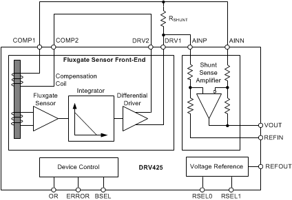
As shown in the Functional Block Diagram section, the DRV425 consists of a magnetic fluxgate sensor with the necessary sensor conditioning and compensation coil to internally close the control loop. The fluxgate sensor is repeatedly driven in and out of saturation and supports hysteresis-free operation with excellent accuracy. The internal compensation coil assures stable gain and high linearity.
The magnetic field (B) is detected by the internal fluxgate sensor in the DRV425. The device integrates the sensor output to assure high-loop gain. The integrator output connects to the built-in differential driver that drives an opposing compensation current through the internal compensation coil. The compensation coil generates an opposite magnetic field that brings the original magnetic field at the sensor back to zero.
The compensation current is proportional to the external magnetic field and its value is 12.2 mA/mT. This compensation current generates a voltage drop across an external shunt resistor, RSHUNT. An integrated difference amplifier with a fixed gain of 4 V/V measures this voltage and generates an output voltage that is referenced to REFIN and is proportional to the magnetic field. The value of the output voltage at the VOUT pin (VVOUT) is calculated using Equation 1:
7.2 Functional Block Diagram
7.3 Feature Description
7.3.1 Fluxgate Sensor Front-End
The following sections describe the functional blocks and features of the integrated fluxgate sensor front-end.
7.3.1.1 Fluxgate Sensor
The fluxgate sensor of the DRV425 is uniquely suited for high-performance magnetic-field sensors because of the high sensitivity, low noise, and low offset of the sensor. The fluxgate principle relies on repeatedly driving the sensor in and out of saturation; therefore, the sensor is free of any significant magnetic hysteresis. The feedback loop accurately drives a compensation current through the integrated compensation coil and drives the magnetic field at the sensor back to zero. This approach supports excellent gain stability and high linearity of the measurement.
The DRV425 package is free of any ferromagnetic materials in order to prevent magnetization by external fields and to obtain accurate and hysteresis-free operation. Select non-magnetizable materials for the printed circuit board (PCB) and passive components in the direct vicinity of the DRV425; see the Layout Guidelines section for more details.
The orientation and the sensitivity axis of the fluxgate sensor is indicated by a dashed line on the top of the package, as shown in Figure 61. Figure 61 also shows the location of the sensor inside the package.
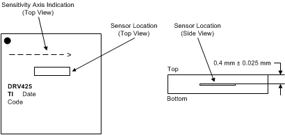 Figure 61. Magnetic Sensitivity Direction of the Integrated Fluxgate Sensor
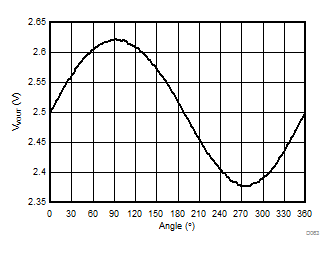
The sensitivity of the fluxgate sensor is a vector function of its sensitivity axis and the magnetic field orientation. Figure 62 shows the output of the DRV425 in dependency of the orientation of the device to a constant magnetic field.
7.3.1.2 Bandwidth
The small-signal bandwidth of the DRV425 is determined by the behavior of the compensation loop versus frequency. The implemented integrator limits the bandwidth of the loop to provide stable response. Use the digital input pin BSEL to select the bandwidth. For a shunt resistor of 22 Ω and BSEL = 0, the bandwidth is 32 kHz; for BSEL = 1, the bandwidth is 47 kHz.
Bandwidth can be reduced by increasing the value of the shunt resistor because the shunt resistor and the compensation coil resistance form a voltage divider. The reduced bandwidth (BW) can be calculated using Equation 2:

where
- RCOIL = internal compensation coil resistance (100 Ω),
- RSHUNT = external shunt resistance, and
- BW22Ω = sensor bandwidth with RSHUNT = 22 Ω (depending on the BSEL setting)
The bandwidth for a given shunt resistor value can also be calculated using the DRV425 System Parameter Calculator, SLOC331. For large magnetic fields (B > 500 μT), the effective bandwidth of the sensor is limited by fluxgate saturation effects. For a magnetic signal with a 2-mT amplitude, the large-signal bandwidth is 10 kHz with BSEL = 0 or 15 kHz with BSEL = 1.
Although the analog output responds slowly to large fields, a magnetic field with a magnitude of 1.6 mT (or higher) beyond the measurement range of the DRV425 triggers the ERROR pin within 4 µs to 6 µs. See the Magnetic Field Range, Overrange Indicator, and Error Flag section for more details.
7.3.1.3 Differential Driver for the Internal Compensation Coil
The differential compensation coil driver provides the current for the internal compensation coil at the DRV1 and DRV2 pins. The driver is capable of sourcing up to ±250 mA with a 5-V supply or up to ±150 mA in 3.3-V mode. The current capability is not internally limited. The actual value of the compensation coil current depends on the magnetic field strength and is limited by the sum of the resistance of the internal compensation coil and the external shunt resistor value. The internal compensation coil resistance depends on temperature (see Figure 17) and must be taken into account when dimensioning the system. Select the value of the shunt resistor to avoid OR pin trip levels in normal operation.
The common-mode voltage of the compensation coil driver outputs is set by the RSEL pins (see the Voltage Reference section). Thus, the common-mode voltage of the shunt-sense amplifier is matched if the internal reference is used.
Consider the polarity of the compensation coil connection to the output of the compensation coil driver. If the polarity is incorrect, then the driver output drives to the power-supply rails, even at low primary-current levels. In this case, interchange the connection of the DRV1 and DRV2 pins to the compensation coil.
7.3.1.4 Magnetic Field Range, Overrange Indicator, and Error Flag
The measurement range of the DRV425 is determined by the amount of current driven into the compensation coil and the output voltage range of the shunt-sense amplifier. The maximum compensation current is limited by the supply voltage and the series resistance of the compensation coil and the shunt.
The magnetic field range is adjusted with the external shunt resistor. The DRV425 System Parameter Calculator, SLOC331 provides the maximum shunt resistor values depending on the supply voltage (VDD) and the selected reference voltage (VREFIN) for various magnetic field ranges.
For proper operation at a maximum field (BMAX), choose a shunt resistor (RSHUNT) using Equation 3

where
- VDD = minimum supply voltage of the DRV425 (V),
- VREFIN = common-mode voltage of the shunt-sense amplifier (V), and
- BMAX = desired magnetic field range (T)
Alternatively, to adjust the output voltage of the DRV425 for a desired maximum voltage (VVOUTMAX), use Equation 4:

where
- VVOUTMAX = desired maximum output voltage at VOUT pin (V), and
- BMAX = desired magnetic field range (T)
To avoid railing of the compensation coil driver, assure that Equation 5 is fulfilled:

where
- BMAX = desired magnetic field range (T),
- RCOIL = compensation coil resistance (Ω),
- VDD = minimum supply voltage of the DRV425 (V), and
- VREFIN = selected internal reference voltage value (V)
The DRV425 System Parameter Calculator, SLOC331 is designed to assist with selecting the system parameters.
The DRV425 offers two diagnostic output pins to detect large fields that exceed the measurement range of the sensor: the overrange indicator (OR) and the ERROR flag.
In normal operation, the DRV425 sensor feedback loop compensates the magnetic field inside the fluxgate to zero. Therefore, a large field inside the fluxgate indicates that the feedback loop is not properly working and the sensor output is invalid. To detect this condition, the ERROR pin is pulled low if the internal field exceeds 1.6 mT. The ERROR output is suppressed for 4 µs to 6 µs to prevent an undesired reaction to transients or noise. For static and slowly varying ambient fields, the ERROR pin triggers when the ambient field exceeds the sensor measurement range by more than 1.6 mT. For dynamic magnetic fields that exceed the sensor bandwidth as specified in the Specifications section, the feedback loop response is too slow to accurately compensate the internal field to zero. Therefore, high-frequency fields can trigger the ERROR pin, even if the ambient field does not exceed the measurement range by 1.6 mT.
In addition, the low-active overrange pin (OR) indicates railing of the output of the shunt-sense amplifier. The OR output is suppressed for 2.5 µs to 3.5 µs to prevent an undesired reaction to transients or noise. The OR pin trip level refers to the output voltage value of the shunt-sense amplifier as specified in the Specifications section. Use Equation 3 and Equation 4 to adjust the OR pin behavior to the specific system-level requirements.
Both the ERROR and OR pins are open-drain outputs that require an external pullup resistor. Connect both pins together with a single pullup resistor to provide a single diagnostic flag, if desired.
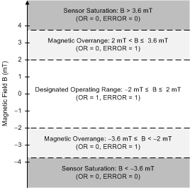
Based on the DRV425 System Parameter Calculator, SLOC331, for a design for a ±2-mT magnetic field input range with a supply of 5 V (±5%), a shunt resistor value of 22 Ω is selected and Figure 63 shows the status of the diagnostic flags in the resulting three operation ranges.
With the proper RSHUNT value, the differential amplifier output rails and activates the overrange flag (OR = 0) when the magnetic field exceeds the designated operating range. For fields that exceed the measurement range of the DRV425 by ≥ 1.6 mT, the fluxgate is permanently saturated and the ERROR pin is pulled low. In this condition, the fluxgate sensor does not provide a valid output value and, therefore, the output VOUT of the DRV425 must be ignored. In applications where the ERROR pin cannot be separately monitored, combining the VOUT and ERROR outputs is recommended (as shown in Figure 64) to indicate a magnetic field outside of the sensor range by pulling the output of the DRV425 to ground.
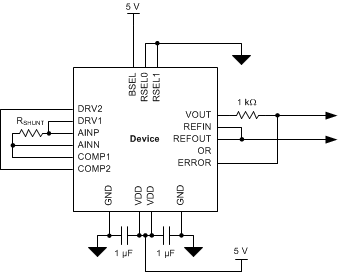 Figure 64. Field Overrange Detection Using a Combined VOUT and ERROR Pin
7.3.2 Shunt-Sense Amplifier
The compensation coil current creates a voltage drop across the external shunt resistor, RSHUNT. The internal differential amplifier senses this voltage drop. This differential amplifier offers wide bandwidth and a high slew rate. Excellent dc stability and accuracy result from a chopping technique. The voltage gain is 4 V/V, set by precisely-matched and thermally-stable internal resistors.
Both the AINN and AINP differential amplifier inputs are connected to the external shunt resistor. This shunt resistor, in series with the internal 10-kΩ input resistors of the shunt sense amplifier, causes an additional gain error. Therefore, for best common-mode rejection performance, place a dummy shunt resistor (R5) with a value higher than the shunt resistor in series with the REFIN pin to restore the matching of both resistor dividers, as shown in Figure 65.
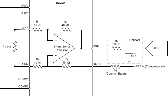 Figure 65. Internal Difference Amplifier with an Example of a Decoupling Filter
For an overall gain of 4 V/V, calculate the value of R5 using Equation 6:

where
- R2 / R1 = R4 / R3 = 4,
- R5 = RSHUNT × 4
If the input signal is large, the amplifier output drives close to the supply rails. The amplifier output is able to drive the input of a successive approximation register (SAR) analog-to-digital converter (ADC). For best performance, add an RC low-pass filter stage between the shunt-sense amplifier output and the ADC input. This filter limits the noise bandwidth and decouples the high-frequency sampling noise of the ADC input from the amplifier output. For filter resistor RF and filter capacitor CF values, see the specific converter recommendations in the respective product data sheet.
The shunt-sense amplifier output drives 100 pF directly and shows a 50% overshoot with a 1-nF capacitance. Filter resistor RF extends the capacitive load range. Note that with an RF of only 20 Ω, the load capacitor must be either less than 1 nF or more than 33 nF to avoid overshoot; with an RF of 50 Ω, this transient area is avoided.
Reference input REFIN is the common-mode voltage node for the output signal VOUT. Use the internal voltage reference of the DRV425 by connecting the REFIN pin to the reference output REFOUT. To avoid mismatch errors, use the same reference voltage for REFIN and the ADC. Alternatively, use an ADC with a pseudo-differential input, with the positive input of the ADC connected to VOUT and the negative input connected to REFIN of the DRV425.
7.3.3 Voltage Reference
The internal precision voltage reference circuit offers low-drift performance at the REFOUT output pin and is used for internal biasing. The reference output is intended to be the common-mode voltage of the output (the VOUT pin) to provide a bipolar signal swing. This low-impedance output tolerates sink and source currents of ±5 mA. However, fast load transients can generate ringing on this line. A small series resistor of a few ohms improves the response, particularly for capacitive loads equal to or greater than 1 μF.
Adjust the value of the voltage reference output to the power supply of the DRV425 using mode selection pins RSEL0 and RSEL1, as shown in Table 1.
Table 1. Reference Output Voltage Selection
| MODE | RSEL1 | RSEL0 | DESCRIPTION |
|---|---|---|---|
| VREFOUT = 2.5 V | 0 | 0 | Use with a sensor module supply of 5 V |
| VREFOUT = 1.65 V | 0 | 1 | Use with a sensor module supply of 3.3 V |
| Ratiometric output | 1 | x | Provides an output centered on VDD / 2 |
In ratiometric output mode, an internal resistor divider divides the power-supply voltage by a factor of two.
7.3.4 Low-Power Operation of the DRV425
In applications with low-bandwidth or low sample-rate requirements, the average power dissipation of the DRV425 can be significantly reduced by powering the device down between measurements. The DRV425 requires 300 μs to fully settle the analog output VOUT, as shown in Figure 66. To minimize power dissipation, the device can be powered down immediately after acquiring the sample by the ADC.
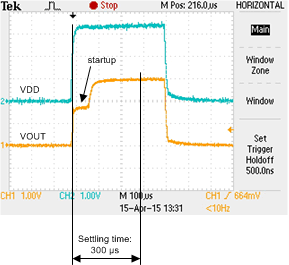 Figure 66. Settling Time of the DRV425 Output VOUT
7.4 Device Functional Modes
The DRV425 is operational when the power supply VDD is applied, as specified in the Specifications section. The DRV425 has no additional functional modes.
