SLVSH22 May 2024 DRV8000-Q1
ADVANCE INFORMATION
- 1
- 1 Features
- 2 Applications
- 3 Description
- 4 Device Comparison
- 5 Pin Configuration and Functions
- 6 Specifications
-
7 Detailed Description
- 7.1 Overview
- 7.2 Functional Block Diagram
- 7.3 External Components
- 7.4
Feature Description
- 7.4.1 Heater MOSFET Driver
- 7.4.2 High-side Drivers
- 7.4.3 Electro-chromic Glass Driver
- 7.4.4 Half-bridge Drivers
- 7.4.5
Gate Drivers
- 7.4.5.1 Input PWM Modes
- 7.4.5.2
Smart Gate Driver - Functional Block
Diagram
- 7.4.5.2.1 Smart Gate Driver
- 7.4.5.2.2 Functional Block Diagram
- 7.4.5.2.3 Slew Rate Control (IDRIVE)
- 7.4.5.2.4 Gate Driver State Machine (TDRIVE)
- 7.4.5.2.5 Propagation Delay Reduction (PDR)
- 7.4.5.2.6 PDR Pre-Charge/Pre-Discharge Control Loop Operation Details
- 7.4.5.2.7 PDR Post-Charge/Post-Discharge Control Loop Operation Details
- 7.4.5.2.8 Detecting Drive and Freewheel MOSFET
- 7.4.5.2.9 Automatic Duty Cycle Compensation (DCC)
- 7.4.5.2.10 Closed Loop Slew Time Control (STC)
- 7.4.5.3 Tripler (Double-Stage) Charge Pump
- 7.4.5.4 Wide Common Mode Differential Current Shunt Amplifier
- 7.4.5.5 Gate Driver Protection Circuits
- 7.4.6 Sense Output (IPROPI)
- 7.4.7
Protection Circuits
- 7.4.7.1 Fault Reset (CLR_FLT)
- 7.4.7.2 DVDD Logic Supply Power on Reset (DVDD_POR)
- 7.4.7.3 PVDD Supply Undervoltage Monitor (PVDD_UV)
- 7.4.7.4 PVDD Supply Overvoltage Monitor (PVDD_OV)
- 7.4.7.5 VCP Charge Pump Undervoltage Lockout (VCP_UV)
- 7.4.7.6 Thermal Clusters
- 7.4.7.7 Watchdog Timer
- 7.4.7.8 Fault Detection and Response Summary Table
- 7.5 Programming
- 8 DRV8000-Q1 Register Map
- 9 DRV8000-Q1_STATUS Registers
- 10DRV8000-Q1_CNFG Registers
- 11DRV8000-Q1_CTRL Registers
- 12Application and Implementation
- 13Device and Documentation Support
- 14Revision History
- 15Mechanical, Packaging, and Orderable Information
7.5.1 SPI Interface
An SPI bus is used to set device configurations, operating parameters, and read out diagnostic information on the DRV8000-Q1 device. The SPI operates in slave mode and connects to a master controller. The SPI input data (SDI) word consists of a 24 bit word, with an 8 bit command and 16 bits of data. The SPI output data (SDO) word for read commands consists of the fault status indication bits and then the register data being accessed for read commands. The SDO word for write commands consists of the command data followed by the existing data in the register being written to. The data sequence between the MCU and the SPI slave driver is shown in Figure 7-36.
 Figure 7-36 SPI Data Frame
A valid frame must meet the following conditions:
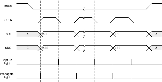
- The SCLK pin should be low when the nSCS pin transitions from high to low and from low to high.
- The nSCS pin should be pulled high between words.
- When the nSCS pin is pulled high, any signals at the SCLK and SDI pins are ignored and the SDO pin is placed in the Hi-Z state.
- Data is captured on the falling edge of SCLK and data is propagated on the rising edge of SCLK.
- The most significant bit (MSB) is shifted in and out first.
- A full 24 SCLK cycles must occur for transaction to be valid.
- If the data word sent to the SDI pin is less than or more than 24 bits, a frame error (SCLK_FLT) occurs and the data word is ignored.
- For a write command, following the 16-bit command data, the existing data in the register being written to is shifted out on the SDO pin starting with fault status byte then 16-bit data .
 Figure 7-37 SPI Slave Timing Diagram