SLVSH22 May 2024 DRV8000-Q1
ADVANCE INFORMATION
- 1
- 1 Features
- 2 Applications
- 3 Description
- 4 Device Comparison
- 5 Pin Configuration and Functions
- 6 Specifications
-
7 Detailed Description
- 7.1 Overview
- 7.2 Functional Block Diagram
- 7.3 External Components
- 7.4
Feature Description
- 7.4.1 Heater MOSFET Driver
- 7.4.2 High-side Drivers
- 7.4.3 Electro-chromic Glass Driver
- 7.4.4 Half-bridge Drivers
- 7.4.5
Gate Drivers
- 7.4.5.1 Input PWM Modes
- 7.4.5.2
Smart Gate Driver - Functional Block
Diagram
- 7.4.5.2.1 Smart Gate Driver
- 7.4.5.2.2 Functional Block Diagram
- 7.4.5.2.3 Slew Rate Control (IDRIVE)
- 7.4.5.2.4 Gate Driver State Machine (TDRIVE)
- 7.4.5.2.5 Propagation Delay Reduction (PDR)
- 7.4.5.2.6 PDR Pre-Charge/Pre-Discharge Control Loop Operation Details
- 7.4.5.2.7 PDR Post-Charge/Post-Discharge Control Loop Operation Details
- 7.4.5.2.8 Detecting Drive and Freewheel MOSFET
- 7.4.5.2.9 Automatic Duty Cycle Compensation (DCC)
- 7.4.5.2.10 Closed Loop Slew Time Control (STC)
- 7.4.5.3 Tripler (Double-Stage) Charge Pump
- 7.4.5.4 Wide Common Mode Differential Current Shunt Amplifier
- 7.4.5.5 Gate Driver Protection Circuits
- 7.4.6 Sense Output (IPROPI)
- 7.4.7
Protection Circuits
- 7.4.7.1 Fault Reset (CLR_FLT)
- 7.4.7.2 DVDD Logic Supply Power on Reset (DVDD_POR)
- 7.4.7.3 PVDD Supply Undervoltage Monitor (PVDD_UV)
- 7.4.7.4 PVDD Supply Overvoltage Monitor (PVDD_OV)
- 7.4.7.5 VCP Charge Pump Undervoltage Lockout (VCP_UV)
- 7.4.7.6 Thermal Clusters
- 7.4.7.7 Watchdog Timer
- 7.4.7.8 Fault Detection and Response Summary Table
- 7.5 Programming
- 8 DRV8000-Q1 Register Map
- 9 DRV8000-Q1_STATUS Registers
- 10DRV8000-Q1_CNFG Registers
- 11DRV8000-Q1_CTRL Registers
- 12Application and Implementation
- 13Device and Documentation Support
- 14Revision History
- 15Mechanical, Packaging, and Orderable Information
7.4.5.2.8 Detecting Drive and Freewheel MOSFET
By default, the PDR loop automatically detects which MOSFET is the drive MOSFET and which MOSFET is the freewheel MOSFET by determining the polarity of the current out of the half-bridge. This is done by measuring the half-bridge VSHx voltage during the dead-time period to determine if the high-side or low-side body diode is conducting. If the current polarity cannot be determined it is assumed that the configured MOSFET through IDIR_MAN_SEL is the drive MOSFET. The automatic freewheel detection can be disabled with the IDIR_MAN bit in register GD_AGD_CNFG. In the manual freewheel modes, the PDR loop relies on the IDIR_MAN_SEL bit in register GD_STC_CNFG to determine which MOSFET is the drive MOSFET and which MOSFET is the freewheel MOSFET. If IDIR_MAN_SEL = 0b, the high-side MOSFET is the drive MOSFET and the low-side MOSFET is the freewheel MOSFET. If IDIR_MAN_SEL = 1b, the low-side MOSFET is the drive MOSFET and high-side MOSFET is the freewheel MOSFET.
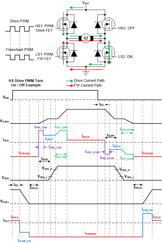
HS Drive PWM Turn On/Off Example shows the high-side MOSFET (HS1) controlling the VSHx switch-node voltage transition and the low-side MOSFET (LS1) acting as the freewheeling MOSFET.
 Figure 7-28 HS Drive PWM Turn On / Off
Example
Figure 7-28 HS Drive PWM Turn On / Off
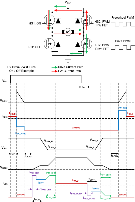
ExampleLS Drive PWM Turn On/Off Example shows the low-side MOSFET (LS2) controlling the VSHx switch-node voltage transition and the high-side MOSFET (HS2) acting as the freewheeling MOSFET.
 Figure 7-29 LS Drive PWM Turn On / Off
Example