SLVSGC3 May   2020 DRV8210P

PRODUCTION DATA  

  1. Features
  2. Applications
  3. Description
  4. Revision History
  5. Device Comparison
  6. Pin Configuration and Functions
  7. Specifications
    1. 7.1 Absolute Maximum Ratings
    2. 7.2 ESD Ratings
    3. 7.3 Recommended Operating Conditions
    4. 7.4 Thermal Information
    5. 7.5 Electrical Characteristics
    6. 7.6 Typical Characteristics
  8. Detailed Description
    1. 8.1 Overview
    2. 8.2 Functional Block Diagram
    3. 8.3 Feature Description
      1. 8.3.1 External Components
      2. 8.3.2 Control Modes
        1. 8.3.2.1 PWM Control
      3. 8.3.3 Protection Circuits
        1. 8.3.3.1 Supply Undervoltage Lockout (UVLO)
        2. 8.3.3.2 OUTx Overcurrent Protection (OCP)
        3. 8.3.3.3 Thermal Shutdown (TSD)
      4. 8.3.4 Pin Diagrams
        1. 8.3.4.1 Logic-Level Inputs
    4. 8.4 Device Functional Modes
      1. 8.4.1 Active Mode
      2. 8.4.2 Low-Power Sleep Mode
      3. 8.4.3 Fault Mode
  9. Application and Implementation
    1. 9.1 Application Information
    2. 9.2 Typical Application
      1. 9.2.1 Full-Bridge Driving
        1. 9.2.1.1 Design Requirements
        2. 9.2.1.2 Detailed Design Procedure
          1. 9.2.1.2.1 Supply Voltage
          2. 9.2.1.2.2 Control Interface
          3. 9.2.1.2.3 Low-Power Operation
        3. 9.2.1.3 Application Curves
      2. 9.2.2 Dual-Coil Relay Driving
        1. 9.2.2.1 Design Requirements
        2. 9.2.2.2 Detailed Design Procedure
          1. 9.2.2.2.1 Supply Voltage
          2. 9.2.2.2.2 Control Interface
          3. 9.2.2.2.3 Low-Power Operation
        3. 9.2.2.3 Application Curves
      3. 9.2.3 Current Sense
        1. 9.2.3.1 Design Requirements
        2. 9.2.3.2 Detailed Design Procedure
          1. 9.2.3.2.1 Shunt Resistor Sizing
    3. 9.3 Current Capability and Thermal Performance
      1. 9.3.1 Power Dissipation and Output Current Capability
      2. 9.3.2 Thermal Performance
        1. 9.3.2.1 Steady-State Thermal Performance
        2. 9.3.2.2 Transient Thermal Performance
  10. 10Power Supply Recommendations
    1. 10.1 Bulk Capacitance
  11. 11Layout
    1. 11.1 Layout Guidelines
    2. 11.2 Layout Example
  12. 12Device and Documentation Support
    1. 12.1 Documentation Support
      1. 12.1.1 Related Documentation
    2. 12.2 Receiving Notification of Documentation Updates
    3. 12.3 Support Resources
    4. 12.4 Trademarks
    5. 12.5 Electrostatic Discharge Caution
    6. 12.6 Glossary
  13. 13Mechanical, Packaging, and Orderable Information

パッケージ・オプション

メカニカル・データ(パッケージ|ピン)
サーマルパッド・メカニカル・データ
発注情報
Control Interface

The PWM interface can be used to drive dual-coil relays. Section 8.3.2.1 describes the PWM control interface. Figure 9-8 and Figure 9-9 show a schematic and timing diagram for driving a dual-coil relay with the PWM interface.
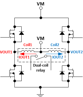
GUID-D57D4663-FE8A-47C1-BC43-38F10F016610-low.gifFigure 9-8 Schematic of dual-coil relay driven by the OUTx H-bridge
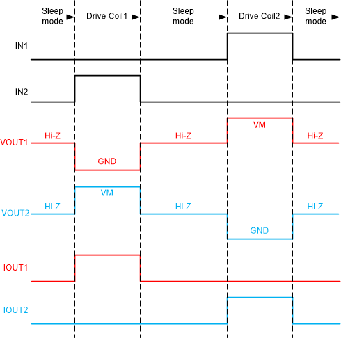
GUID-F0552D3C-2210-4D5E-B2B7-DC84417542B3-low.gifFigure 9-9 Timing diagram for driving a dual-coil relay with PWM interface

Table 9-3 shows the logic table for the PWM interface. The descriptions in this table reflect how the input and output states drive the dual coil relay. When Coil1 is driven (OUT1 voltage is at GND), The voltage at OUT2 will go to VM. Because the center tap of the relay is also at VM, no current flows through Coil2. The same is true when Coil2 is driven; Coil1 shorts to VM. The body diodes of the high-side FETs act as freewheeling diodes, so extra external diodes are not needed. Figure 9-10 shows oscilloscope traces for this application.

Table 9-3 PWM control table for dual-coil relay driving
IN1 IN2 OUT1 OUT2 DESCRIPTION
0 0 Hi-Z Hi-Z Outputs disabled (H-Bridge Hi-Z)
0 1 L H Drive Coil1
1 0 H L Drive Coil2
1 1 L L Drive Coil1 and Coil2 (invalid state for a dual-coil latching relay)