JAJSJS9B July   2023  – October 2024 DRV8262

PRODUCTION DATA  

  1.   1
  2. 特長
  3. アプリケーション
  4. 概要
  5. Pin Configuration and Functions
  6. Specifications
    1. 5.1 Absolute Maximum Ratings
    2. 5.2 ESD Ratings
    3. 5.3 Recommended Operating Conditions
    4. 5.4 Thermal Information
      1. 5.4.1 Transient Thermal Impedance & Current Capability
    5. 5.5 Electrical Characteristics
    6. 5.6 Typical Characteristics
  7. Detailed Description
    1. 6.1  Overview
    2. 6.2  Functional Block Diagram
    3. 6.3  Feature Description
    4. 6.4  Device Operational Modes
      1. 6.4.1 Dual H-Bridge Mode (MODE1 = 0)
      2. 6.4.2 Single H-Bridge Mode (MODE1 = 1)
    5. 6.5  Current Sensing and Regulation
      1. 6.5.1 Current Sensing and Feedback
      2. 6.5.2 Current Regulation
        1. 6.5.2.1 Mixed Decay
        2. 6.5.2.2 Smart tune Dynamic Decay
      3. 6.5.3 Current Sensing with External Resistor
    6. 6.6  Charge Pump
    7. 6.7  Linear Voltage Regulator
    8. 6.8  VCC Voltage Supply
    9. 6.9  Logic Level, Tri-Level and Quad-Level Pin Diagrams
    10. 6.10 Protection Circuits
      1. 6.10.1 VM Undervoltage Lockout (UVLO)
      2. 6.10.2 VCP Undervoltage Lockout (CPUV)
      3. 6.10.3 Logic Supply Power on Reset (POR)
      4. 6.10.4 Overcurrent Protection (OCP)
      5. 6.10.5 Thermal Shutdown (OTSD)
      6. 6.10.6 nFAULT Output
      7. 6.10.7 Fault Condition Summary
    11. 6.11 Device Functional Modes
      1. 6.11.1 Sleep Mode
      2. 6.11.2 Operating Mode
      3. 6.11.3 nSLEEP Reset Pulse
      4. 6.11.4 Functional Modes Summary
  8. Application and Implementation
    1. 7.1 Application Information
      1. 7.1.1 Driving Brushed-DC Motors
        1. 7.1.1.1 Brushed-DC Motor Driver Typical Application
        2. 7.1.1.2 Power Loss Calculations - Dual H-bridge
        3. 7.1.1.3 Power Loss Calculations - Single H-bridge
        4. 7.1.1.4 Junction Temperature Estimation
        5. 7.1.1.5 Application Performance Plots
      2. 7.1.2 Driving Stepper Motors
        1. 7.1.2.1 Stepper Driver Typical Application
        2. 7.1.2.2 Power Loss Calculations
        3. 7.1.2.3 Junction Temperature Estimation
      3. 7.1.3 Driving Thermoelectric Coolers (TEC)
    2. 7.2 Power Supply Recommendations
      1. 7.2.1 Bulk Capacitance
      2. 7.2.2 Power Supplies
    3. 7.3 Layout
      1. 7.3.1 Layout Guidelines
      2. 7.3.2 Layout Example
  9. Package Thermal Considerations
    1. 8.1 DDW Package
      1. 8.1.1 Thermal Performance
        1. 8.1.1.1 Steady-State Thermal Performance
        2. 8.1.1.2 Transient Thermal Performance
    2. 8.2 DDV Package
    3. 8.3 PCB Material Recommendation
  10. Device and Documentation Support
    1. 9.1 Documentation Support
      1. 9.1.1 Related Documentation
    2. 9.2 ドキュメントの更新通知を受け取る方法
    3. 9.3 サポート・リソース
    4. 9.4 Trademarks
    5. 9.5 静電気放電に関する注意事項
    6. 9.6 用語集
  11. 10Revision History
  12. 11Mechanical, Packaging, and Orderable Information
    1. 11.1 Tape and Reel Information

パッケージ・オプション

メカニカル・データ(パッケージ|ピン)
サーマルパッド・メカニカル・データ
発注情報

nFAULT Output

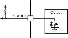
The nFAULT pin has an open-drain output and should be pulled up to a 5V, 3.3V, or 1.8V supply. When a fault is detected, the nFAULT pin will be logic low. nFAULT pin will be high after power-up. For a 5V pullup, the nFAULT pin can be tied to the DVDD pin with a resistor. For a 3.3V or 1.8V pullup, an external supply must be used.
DRV8262 nFAULT PinFigure 6-15 nFAULT Pin