JAJSFH4B November   2017  – July 2018 DRV8304

UNLESS OTHERWISE NOTED, this document contains PRODUCTION DATA.  

  1. 特長
  2. アプリケーション
  3. 概要
    1.     概略回路図
  4. 改訂履歴
  5. Pin Configuration and Functions
    1.     Pin Functions
  6. Specifications
    1. 6.1 Absolute Maximum Ratings
    2. 6.2 ESD Ratings
    3. 6.3 Recommended Operating Conditions
    4. 6.4 Thermal Information
    5. 6.5 Electrical Characteristics
    6. 6.6 Timing Requirements
    7. 6.7 Typical Characteristics
  7. Detailed Description
    1. 7.1 Overview
    2. 7.2 Functional Block Diagram
    3. 7.3 Feature Description
      1. 7.3.1 3-Phase Smart Gate Drivers
        1. 7.3.1.1 PWM Control Modes
          1. 7.3.1.1.1 6x PWM Mode (PWM_MODE = 00b or MODE Pin Tied to AGND)
          2. 7.3.1.1.2 3x PWM Mode (PWM_MODE = 01b or MODE Pin = 47 kΩ to AGND)
          3. 7.3.1.1.3 1x PWM Mode (PWM_MODE = 10b or MODE Pin = Hi-Z)
          4. 7.3.1.1.4 Independent PWM Mode (PWM_MODE = 11b or MODE Pin Tied to DVDD)
        2. 7.3.1.2 Device Interface Modes
          1. 7.3.1.2.1 Serial Peripheral Interface (SPI)
          2. 7.3.1.2.2 Hardware Interface
        3. 7.3.1.3 Gate Driver Voltage Supplies
        4. 7.3.1.4 Smart Gate-Drive Architecture
          1. 7.3.1.4.1 IDRIVE: MOSFET Slew-Rate Control
          2. 7.3.1.4.2 TDRIVE: MOSFET Gate Drive Control
          3. 7.3.1.4.3 Gate Drive Clamp
          4. 7.3.1.4.4 Propagation Delay
          5. 7.3.1.4.5 MOSFET VDS Monitors
          6. 7.3.1.4.6 VDRAIN Sense Pin
      2. 7.3.2 DVDD Linear Voltage Regulator
      3. 7.3.3 Pin Diagrams
      4. 7.3.4 Low-Side Current-Shunt Amplifiers
        1. 7.3.4.1 Bidirectional Current Sense Operation
        2. 7.3.4.2 Unidirectional Current Sense Operation (SPI only)
        3. 7.3.4.3 Offset Calibration
      5. 7.3.5 Gate-Driver Protection Circuits
        1. 7.3.5.1 VM Supply Undervoltage Lockout (UVLO)
        2. 7.3.5.2 VCP Charge-Pump Undervoltage Lockout (CPUV)
        3. 7.3.5.3 MOSFET VDS Overcurrent Protection (VDS_OCP)
          1. 7.3.5.3.1 VDS Latched Shutdown (OCP_MODE = 00b)
          2. 7.3.5.3.2 VDS Automatic Retry (OCP_MODE = 01b)
          3. 7.3.5.3.3 VDS Report Only (OCP_MODE = 10b)
          4. 7.3.5.3.4 VDS Disabled (OCP_MODE = 11b)
        4. 7.3.5.4 VSENSE Overcurrent Protection (SEN_OCP)
          1. 7.3.5.4.1 VSENSE Latched Shutdown (OCP_MODE = 00b)
          2. 7.3.5.4.2 VSENSE Automatic Retry (OCP_MODE = 01b)
          3. 7.3.5.4.3 VSENSE Report Only (OCP_MODE = 10b)
          4. 7.3.5.4.4 VSENSE Disabled (OCP_MODE = 11b or DIS_SEN = 1b)
        5. 7.3.5.5 Gate Driver Fault (GDF)
        6. 7.3.5.6 Thermal Warning (OTW)
        7. 7.3.5.7 Thermal Shutdown (OTSD)
    4. 7.4 Device Functional Modes
      1. 7.4.1 Gate Driver Functional Modes
        1. 7.4.1.1 Sleep Mode
        2. 7.4.1.2 Operating Mode
        3. 7.4.1.3 Fault Reset (CLR_FLT or ENABLE Reset Pulse)
    5. 7.5 Programming
      1. 7.5.1 SPI Communication
        1. 7.5.1.1 SPI
          1. 7.5.1.1.1 SPI Format
    6. 7.6 Register Maps
      1. Table 1. DRV8304S Register Map
      2. 7.6.1     Status Registers (DRV8304S Only)
        1. 7.6.1.1 Fault Status Register 1 (Address = 0x00) [reset = 0x00]
          1. Table 11. Fault Status Register 1 Field Descriptions
        2. 7.6.1.2 Fault Status Register 2 (Address = 0x01) [reset = 0x00]
          1. Table 12. Fault Status Register 2 Field Descriptions
      3. 7.6.2     Control Registers (DRV8304S Only)
        1. 7.6.2.1 Driver Control Register (Address = 0x02) [reset = 0x00]
          1. Table 14. Driver Control Field Descriptions
        2. 7.6.2.2 Gate Drive HS Register (Address = 0x03) [reset = 0x377]
          1. Table 15. Gate Drive HS Field Descriptions
        3. 7.6.2.3 Gate Drive LS Register (Address = 0x04) [reset = 0x777]
          1. Table 16. Gate Drive LS Register Field Descriptions
        4. 7.6.2.4 OCP Control Register (Address = 0x05) [reset = 0x145]
          1. Table 17. OCP Control Field Descriptions
        5. 7.6.2.5 CSA Control Register (Address = 0x06) [reset = 0x283]
          1. Table 18. CSA Control Field Descriptions
  8. Application and Implementation
    1. 8.1 Application Information
    2. 8.2 Typical Application
      1. 8.2.1 Primary Application
        1. 8.2.1.1 Design Requirements
        2. 8.2.1.2 Detailed Design Procedure
          1. 8.2.1.2.1 External MOSFET Support
            1. 8.2.1.2.1.1 Example
          2. 8.2.1.2.2 IDRIVE Configuration
            1. 8.2.1.2.2.1 Example
          3. 8.2.1.2.3 VDS Overcurrent Monitor Configuration
            1. 8.2.1.2.3.1 Example
          4. 8.2.1.2.4 Sense-Amplifier Bidirectional Configuration
            1. 8.2.1.2.4.1 Example
        3. 8.2.1.3 Application Curves
      2. 8.2.2 Alternative Application
        1. 8.2.2.1 Design Requirements
        2. 8.2.2.2 Detailed Design Procedure
          1. 8.2.2.2.1 Sense-Amplifier Unidirectional Configuration
            1. 8.2.2.2.1.1 Example
  9. Power Supply Recommendations
    1. 9.1 Bulk Capacitance Sizing
  10. 10Layout
    1. 10.1 Layout Guidelines
    2. 10.2 Layout Example
  11. 11デバイスおよびドキュメントのサポート
    1. 11.1 デバイス・サポート
      1. 11.1.1 デバイスの項目表記
    2. 11.2 ドキュメントのサポート
      1. 11.2.1 関連資料
    3. 11.3 ドキュメントの更新通知を受け取る方法
    4. 11.4 コミュニティ・リソース
    5. 11.5 商標
    6. 11.6 静電気放電に関する注意事項
    7. 11.7 Glossary
  12. 12メカニカル、パッケージ、および注文情報

パッケージ・オプション

デバイスごとのパッケージ図は、PDF版データシートをご参照ください。

メカニカル・データ(パッケージ|ピン)
  • RHA|40
サーマルパッド・メカニカル・データ
発注情報

Pin Diagrams

Figure 25 shows the input structure for the logic-level pins, INHx, INLx, CAL, nSCS, SCLK, and SDI. The input can be driven with a voltage or external resistor.
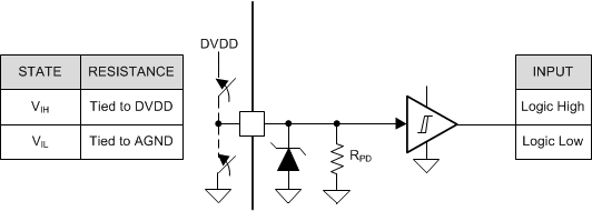
DRV8304 drv8304_logic_level_input_pin_structure.gifFigure 25. Logic-Level Input Pin Structure (INHx, INLx, CAL, nSCS, SCLK, and SDI)

Figure 26 shows the input structure for the logic-level ENABLE pin. The input can be driven with a voltage or external resistor. The ENABLE pin is latched when the device is powered-up.
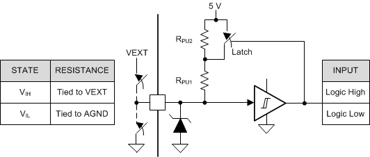
DRV8304 drv8304_logic-level-input-pin-structure_enable.gifFigure 26. Logic-Level Input Pin Structure (ENABLE)

Figure 27 shows the structure of the four-level input pins, MODE and GAIN, on the hardware interface device. The input can be set with an external resistor. The MODE and GAIN pins are latched when the device is powered-up.
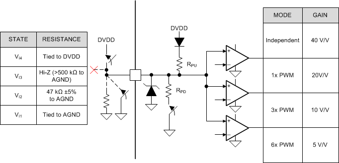
DRV8304 drv8304_four_level_input_pin_struct.gifFigure 27. Four-Level Input Pin Structure (MODE and GAIN)

Figure 28 shows the structure of the seven-level input pins, IDRIVE and VDS, on the hardware interface device. The input can be set with an external resistor. The IDRIVE and VDS pins are latched when the device is powered-up.
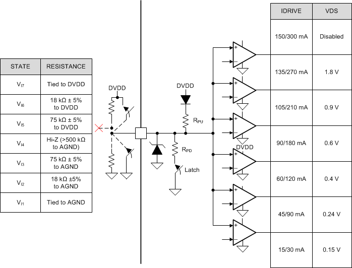
DRV8304 drv8304_seven_level_input_pin_structure.gifFigure 28. Seven-Level Input Pin Structure (IDRIVE and VDS)

Figure 29 shows the structure of the open-drain output pin, nFAULT. The open-drain output requires an external pullup resistor to function properly.
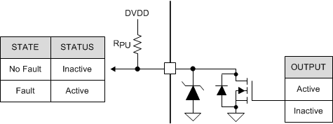
DRV8304 drv8304-open-drain.gifFigure 29. Open-Drain Output Pin Structure