JAJSFH4B November 2017 – July 2018 DRV8304
UNLESS OTHERWISE NOTED, this document contains PRODUCTION DATA.
- 1 特長
- 2 アプリケーション
- 3 概要
- 4 改訂履歴
- 5 Pin Configuration and Functions
- 6 Specifications
-
7 Detailed Description
- 7.1 Overview
- 7.2 Functional Block Diagram
- 7.3
Feature Description
- 7.3.1 3-Phase Smart Gate Drivers
- 7.3.2 DVDD Linear Voltage Regulator
- 7.3.3 Pin Diagrams
- 7.3.4 Low-Side Current-Shunt Amplifiers
- 7.3.5 Gate-Driver Protection Circuits
- 7.4 Device Functional Modes
- 7.5 Programming
- 7.6
Register Maps
- Table 1. DRV8304S Register Map
- 7.6.1 Status Registers (DRV8304S Only)
- 7.6.2
Control Registers (DRV8304S Only)
- 7.6.2.1 Driver Control Register (Address = 0x02) [reset = 0x00]
- 7.6.2.2 Gate Drive HS Register (Address = 0x03) [reset = 0x377]
- 7.6.2.3 Gate Drive LS Register (Address = 0x04) [reset = 0x777]
- 7.6.2.4 OCP Control Register (Address = 0x05) [reset = 0x145]
- 7.6.2.5 CSA Control Register (Address = 0x06) [reset = 0x283]
- 8 Application and Implementation
- 9 Power Supply Recommendations
- 10Layout
- 11デバイスおよびドキュメントのサポート
- 12メカニカル、パッケージ、および注文情報
パッケージ・オプション
デバイスごとのパッケージ図は、PDF版データシートをご参照ください。
メカニカル・データ(パッケージ|ピン)
- RHA|40
サーマルパッド・メカニカル・データ
- RHA|40
発注情報
7.3.4.1 Bidirectional Current Sense Operation
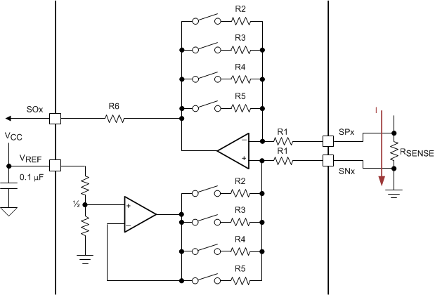
The SOx pin on the DRV8304 outputs an analog voltage equal to the voltage across the SPx and SNx pins multiplied by the gain setting (GCSA) as shown in Figure 30. The gain setting is adjustable between four different levels (5 V/V, 10 V/V, 20 V/V, and 40 V/V). Use Equation 3 to calculate the current through the shunt resistor.

 Figure 30. Bidirectional Current-Sense Configuration
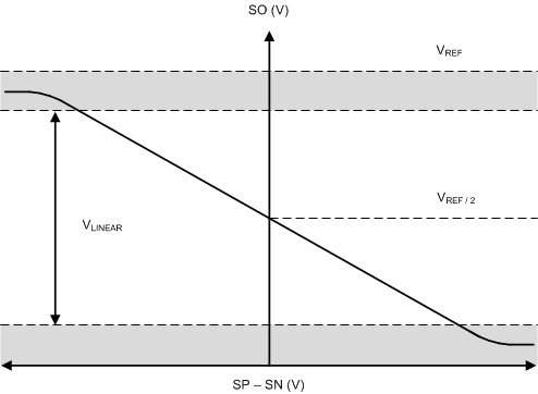
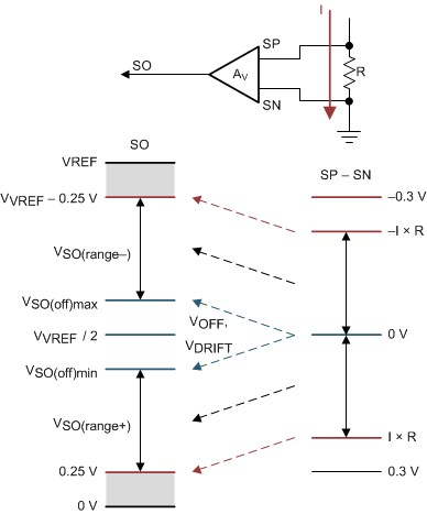
 Figure 31 and Figure 32 show the detail of the amplifier operational range. In bi-directional operation, the amplifier output for 0-V input is set at VREF / 2. Any change in the differential input results in a corresponding change in the output times the CSA_GAIN factor. The amplifier has a defined linear region in which it can maintain operation.
 Figure 31. Bidirectional Current-Sense Output
  Figure 32. Bidirectional Current Sense Regions