JAJSSZ1 December 2023 DRV8334
PRODUCTION DATA
- 1
- 1 特長
- 2 アプリケーション
- 3 概要
- 4 Revision History
- 5 Pin Configuration and Functions
- 6 Specification
-
7 Detailed Description
- 7.1 Overview
- 7.2 Functional Block Diagram
- 7.3
Feature Description
- 7.3.1 Three BLDC Gate Drivers
- 7.3.2 Low-Side Current Sense Amplifiers
- 7.3.3 Gate Driver Shutdown
- 7.3.4
Gate Driver Protective Circuits
- 7.3.4.1 PVDD Supply Undervoltage Lockout (PVDD_UV)
- 7.3.4.2 GVDD Undervoltage Lockout (GVDD_UV)
- 7.3.4.3 BST Undervoltage Lockout (BST_UV)
- 7.3.4.4 MOSFET VDS Overcurrent Protection (VDS_OCP)
- 7.3.4.5 VSENSE Overcurrent Protection (SEN_OCP)
- 7.3.4.6 Phase Comparators
- 7.3.4.7 Thermal Shutdown (OTSD)
- 7.3.4.8 Thermal Warning (OTW)
- 7.3.4.9 OTP CRC
- 7.3.4.10 SPI Watchdog Timer
- 7.4 Device Functional Modes
- 7.5 Programming
- 7.6 Register Maps
- 8 Application and Implementation
- 9 Layout
- 10Device and Documentation Support
- 11Mechanical, Packaging, and Orderable Information
7.3.1.1.4 1x PWM Mode
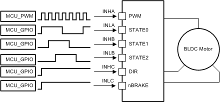
In 1x PWM mode, the device uses 6-step block commutation tables that are stored internally. This feature allows for a three-phase BLDC motor to be controlled using one PWM sourced from a simple controller. The PWM is applied on the INHA pin and determines the output frequency and duty cycle of the half-bridges.
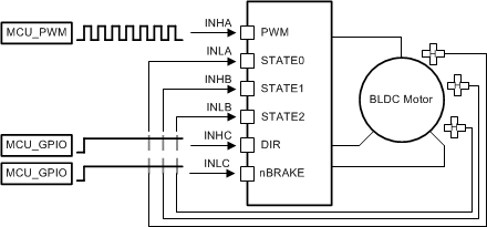
The half-bridge output states are managed by the INLA, INHB, and INLB pins which are used as state logic inputs. The state inputs can be controlled by an external controller or connected directly to the digital outputs of the Hall effect sensor from the motor (INLA = HALL_A, INHB = HALL_B, INLB = HALL_C). The 1x PWM mode usually operates with synchronous rectification (low-side MOSFET recirculation).
The INHC input controls the direction through the 6-step commutation table which is used to change the direction of the motor when Hall effect sensors are directly controlling the state of the INLA, INHB, and INLB inputs. Tie the INHC pin low if this feature is not required.
The INLC input brakes the motor by turning off all high-side MOSFETs and turning on all low-side MOSFETs when the INLC pin is pulled low. This brake is independent of the state of the other input pins. Tie the INLC pin high if this feature is not required.
| LOGIC AND HALL INPUTS | GATE DRIVE OUTPUTS(1) | ||||||||||||
|---|---|---|---|---|---|---|---|---|---|---|---|---|---|
| STATE | INHC = 0 | INHC = 1 | PHASE A | PHASE B | PHASE C | DESCRIPTION | |||||||
| INLA | INHB | INLB | INLA | INHB | INLB | GHA | GLA | GHB | GLB | GHC | GLC | ||
| Stop | 0 | 0 | 0 | 0 | 0 | 0 | L | L | L | L | L | L | Stop |
| Align | 1 | 1 | 1 | 1 | 1 | 1 | PWM | !PWM | L | H | L | H | Align |
| 1 | 1 | 1 | 0 | 0 | 0 | 1 | L | L | PWM | !PWM | L | H | B → C |
| 2 | 1 | 0 | 0 | 0 | 1 | 1 | PWM | !PWM | L | L | L | H | A → C |
| 3 | 1 | 0 | 1 | 0 | 1 | 0 | PWM | !PWM | L | H | L | L | A → B |
| 4 | 0 | 0 | 1 | 1 | 1 | 0 | L | L | L | H | PWM | !PWM | C → B |
| 5 | 0 | 1 | 1 | 1 | 0 | 0 | L | H | L | L | PWM | !PWM | C → A |
| 6 | 0 | 1 | 0 | 1 | 0 | 1 | L | H | PWM | !PWM | L | L | B → A |
| LOGIC AND HALL INPUTS | GATE DRIVE OUTPUTS | ||||||||||||
|---|---|---|---|---|---|---|---|---|---|---|---|---|---|
| STATE | INHC = 0 | INHC = 1 | PHASE A | PHASE B | PHASE C | DESCRIPTION | |||||||
| INLA | INHB | INLB | INLA | INHB | INLB | GHA | GLA | GHB | GLB | GHC | GLC | ||
| Stop | 0 | 0 | 0 | 0 | 0 | 0 | L | L | L | L | L | L | Stop |
| Align | 1 | 1 | 1 | 1 | 1 | 1 | PWM | L | L | H | L | H | Align |
| 1 | 1 | 1 | 0 | 0 | 0 | 1 | L | L | PWM | L | L | H | B → C |
| 2 | 1 | 0 | 0 | 0 | 1 | 1 | PWM | L | L | L | L | H | A → C |
| 3 | 1 | 0 | 1 | 0 | 1 | 0 | PWM | L | L | H | L | L | A → B |
| 4 | 0 | 0 | 1 | 1 | 1 | 0 | L | L | L | H | PWM | L | C → B |
| 5 | 0 | 1 | 1 | 1 | 0 | 0 | L | H | L | L | PWM | L | C → A |
| 6 | 0 | 1 | 0 | 1 | 0 | 1 | L | H | PWM | L | L | L | B → A |
Figure 7-2 and Figure 7-3 show the different possible configurations in 1x PWM mode.
 Figure 7-2 1x PWM—Simple Controller
 Figure 7-3 1x PWM—Hall Effect Sensor