SLVSHQ2 December   2024 DRV8351-SEP

PRODUCTION DATA  

  1.   1
  2. Features
  3. Applications
  4. Description
  5. Device Comparison Table
  6. Pin Configuration and Functions
  7. Specifications
    1. 6.1 Absolute Maximum Ratings
    2. 6.2 ESD Ratings Comm
    3. 6.3 Recommended Operating Conditions
    4. 6.4 Thermal Information
    5. 6.5 Electrical Characteristics
    6. 6.6 Timing Diagrams
    7. 6.7 Typical Characteristics
  8. Detailed Description
    1. 7.1 Overview
    2. 7.2 Functional Block Diagram
    3. 7.3 Feature Description
      1. 7.3.1 Three BLDC Gate Drivers
        1. 7.3.1.1 Gate Driver Timings
          1. 7.3.1.1.1 Propagation Delay
          2. 7.3.1.1.2 Deadtime and Cross-Conduction Prevention
        2. 7.3.1.2 Mode (Inverting and non inverting INLx)
      2. 7.3.2 Pin Diagrams
      3. 7.3.3 Gate Driver Protective Circuits
        1. 7.3.3.1 VBSTx Undervoltage Lockout (BSTUV)
        2. 7.3.3.2 GVDD Undervoltage Lockout (GVDDUV)
    4. 7.4 Device Functional Modes
  9. Application and Implementation
    1. 8.1 Application Information
    2. 8.2 Typical Application
      1. 8.2.1 Design Requirements
      2. 8.2.2 Bootstrap Capacitor and GVDD Capacitor Selection
      3. 8.2.3 Application Curves
  10. Power Supply Recommendations
  11. 10Layout
    1. 10.1 Layout Guidelines
    2. 10.2 Layout Example
  12. 11Device and Documentation Support
    1. 11.1 Receiving Notification of Documentation Updates
    2. 11.2 Support Resources
    3. 11.3 Trademarks
    4. 11.4 Electrostatic Discharge Caution
    5. 11.5 Glossary
  13. 12Revision History
  14. 13Mechanical, Packaging, and Orderable Information

パッケージ・オプション

メカニカル・データ(パッケージ|ピン)
サーマルパッド・メカニカル・データ
発注情報
Deadtime and Cross-Conduction Prevention

In the DRV8351-SEP, high-side and low-side inputs operate independently, with an exception to prevent cross conduction when high and low side are turned ON at the same time. The DRV8351-SEP turns OFF high-side and low-side output to prevent shoot through when both high-side and low-side inputs are at logic HIGH at the same time.

In DRV8351D-SEP, fixed deadtime of 200 ns (typical value) is inserted to prevent high and low side gate output turning ON at same time.
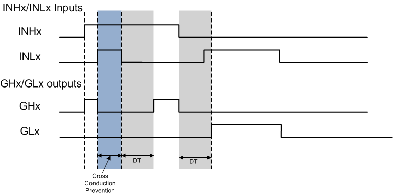
DRV8351-SEP Cross Conduction Prevention and Deadtime InsertionFigure 7-2 Cross Conduction Prevention and Deadtime Insertion