SLVSHQ2 December   2024 DRV8351-SEP

PRODUCTION DATA  

  1.   1
  2. Features
  3. Applications
  4. Description
  5. Device Comparison Table
  6. Pin Configuration and Functions
  7. Specifications
    1. 6.1 Absolute Maximum Ratings
    2. 6.2 ESD Ratings Comm
    3. 6.3 Recommended Operating Conditions
    4. 6.4 Thermal Information
    5. 6.5 Electrical Characteristics
    6. 6.6 Timing Diagrams
    7. 6.7 Typical Characteristics
  8. Detailed Description
    1. 7.1 Overview
    2. 7.2 Functional Block Diagram
    3. 7.3 Feature Description
      1. 7.3.1 Three BLDC Gate Drivers
        1. 7.3.1.1 Gate Driver Timings
          1. 7.3.1.1.1 Propagation Delay
          2. 7.3.1.1.2 Deadtime and Cross-Conduction Prevention
        2. 7.3.1.2 Mode (Inverting and non inverting INLx)
      2. 7.3.2 Pin Diagrams
      3. 7.3.3 Gate Driver Protective Circuits
        1. 7.3.3.1 VBSTx Undervoltage Lockout (BSTUV)
        2. 7.3.3.2 GVDD Undervoltage Lockout (GVDDUV)
    4. 7.4 Device Functional Modes
  9. Application and Implementation
    1. 8.1 Application Information
    2. 8.2 Typical Application
      1. 8.2.1 Design Requirements
      2. 8.2.2 Bootstrap Capacitor and GVDD Capacitor Selection
      3. 8.2.3 Application Curves
  10. Power Supply Recommendations
  11. 10Layout
    1. 10.1 Layout Guidelines
    2. 10.2 Layout Example
  12. 11Device and Documentation Support
    1. 11.1 Receiving Notification of Documentation Updates
    2. 11.2 Support Resources
    3. 11.3 Trademarks
    4. 11.4 Electrostatic Discharge Caution
    5. 11.5 Glossary
  13. 12Revision History
  14. 13Mechanical, Packaging, and Orderable Information

パッケージ・オプション

メカニカル・データ(パッケージ|ピン)
サーマルパッド・メカニカル・データ
発注情報

Mode (Inverting and non inverting INLx)

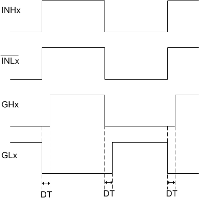
The DRV8351-SEP has flexibility of accepting different kind of inputs on INLx. In DRV8351-SEP, there are different device options available for inverting and non inverting inputs (see Section 4).
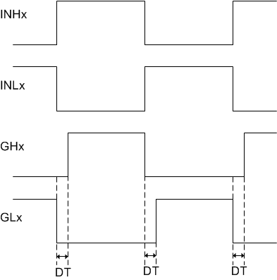
DRV8351-SEP Non-Inverted INLx inputsFigure 7-3 Non-Inverted INLx inputs
DRV8351-SEP Inverted INLx inputsFigure 7-4 Inverted INLx inputs