JAJSKV6D August 2020 – April 2024 DRV8714-Q1 , DRV8718-Q1
PRODMIX
- 1
- 1 特長
- 2 アプリケーション
- 3 概要
- 4 Device Comparison Table
- 5 Pin Configuration and Functions
- 6 Specifications
-
7 Detailed Description
- 7.1 Overview
- 7.2 Functional Block Diagram
- 7.3
Feature Description
- 7.3.1 External Components
- 7.3.2 Device Interface Variants
- 7.3.3 Input PWM Control Modes
- 7.3.4 Smart Gate Driver
- 7.3.5 Tripler (Dual-Stage) Charge Pump
- 7.3.6 Wide Common-Mode Current Shunt Amplifiers
- 7.3.7 Pin Diagrams
- 7.3.8
Protection and Diagnostics
- 7.3.8.1 Gate Driver Disable (DRVOFF/nFLT and EN_DRV)
- 7.3.8.2 Low IQ Powered Off Braking (POB, BRAKE)
- 7.3.8.3 Fault Reset (CLR_FLT)
- 7.3.8.4 DVDD Logic Supply Power on Reset (DVDD_POR)
- 7.3.8.5 PVDD Supply Undervoltage Monitor (PVDD_UV)
- 7.3.8.6 PVDD Supply Overvoltage Monitor (PVDD_OV)
- 7.3.8.7 VCP Charge Pump Undervoltage Lockout (VCP_UV)
- 7.3.8.8 MOSFET VDS Overcurrent Protection (VDS_OCP)
- 7.3.8.9 Gate Driver Fault (VGS_GDF)
- 7.3.8.10 Thermal Warning (OTW)
- 7.3.8.11 Thermal Shutdown (OTSD)
- 7.3.8.12 Offline Short Circuit and Open Load Detection (OOL and OSC)
- 7.3.8.13 Watchdog Timer
- 7.3.8.14 Fault Detection and Response Summary Table
- 7.4 Device Functional Modes
- 7.5 Programming
- 8 Register Maps
- 9 Application Implementation
- 10Device Documentation and Support
- 11Revision History
- 12Mechanical, Packaging, and Orderable Information
パッケージ・オプション
メカニカル・データ(パッケージ|ピン)
- RVJ|56
サーマルパッド・メカニカル・データ
- RVJ|56
発注情報
7.3.3.1.2 DRV8714-Q1 Half-Bridge Control
The DRV8714-Q1 controls the four half-bridge gate drivers through a combination of direct PWM, PWM multiplexers, and SPI control registers. The half-bridge control mode can be enabled by setting BRG_MODE = 00b on SPI interface variants or the MODE pin to level 1 on H/W interface variants. On SPI interface variants, the HBx_CTRL (half-bridge control) SPI register is used to control the half-bridge gate driver output state. The different control states for the gate drivers are shown in Table 7-6. Any unused half-bridge drivers should be left disconnected and in the high-impedance (Hi-Z) output state. On H/W interface variants, the device defaults to direct PWM control from the associated INx/ENx input pins.
The DRV8714-Q1 PWM inputs pins (IN1/EN1, IN2/PH1. IN3/EN2, IN4/PH2) can be used to set the PWM frequency and duty cycle for the assigned output. If high frequency or precise duty cycle PWM control is not required, the four half-bridge gate drivers can be controlled directly through the HBx_CTRL SPI control register on SPI interface variants.
The DRV8714-Q1 can also be used to control individual high-side or low-side external MOSFETs instead of a half-bridge. In this setup, simply leave the unused GHx/GLx driver of the half-bridge disconnected. Only passive freewheeling should be utilized if PWM control is needed in this setup.
| HBx_CTRL (1-4) | Gate Driver State | GHx (1-4) | GLx (1-4) | SHx (1-4) |
|---|---|---|---|---|
| 00b | High Impedance (Hi-Z) | L | L | Hi-Z |
| 01b | Drive Low-Side (L) | L | H | L |
| 10b | Drive High-Side (H) | H | L | H |
| 11b | Drive PWM (PWM) | Table 7-8 | Table 7-8 | Table 7-8 |
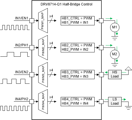
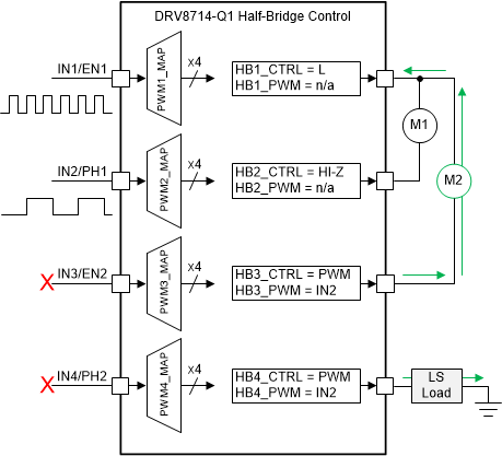
In PWM control mode, the half-bridge gate drivers can be controlled directly by any of 4 independent PWM control inputs (IN1, IN2, IN3, IN4) as shown in Table 7-4. On H/W interface variants, the PWM control inputs map directly to their associated output number.
PWM mapping helps reduce the number of required PWM resources and pins from the external controller when utilizing motor groups or zone control schemes while still allowing for fine PWM frequency and duty cycle control. Each PWM input pin can be mapped to as many half-bridge drivers as desired. The input PWM signal can actively drive the high-side or low-side MOSFET of the half-bridge (based on PWMx_HL control register), with the opposite MOSFET in the half-bridge being controlled accordingly based on the freewheeling setting. Either active or passive freewheeling can be configured by the PWMx_FW control register. On H/W interface variants, the device is configured for high-side PWM drive with active freewheeling.
The following steps should be taken to modify the PWM mapping scheme during driver operation.
- Set active half-bridge to Hi-Z mode through HBx_CTRL.
- Set new target half-bridge to Hi-Z mode through HBx_CTRL.
- HBx_PWM mapping should be updated from the old target to the new target half-bridge.
- Set new target half-bridge drive MOSFET (PWMx_HL) and freewheeling settings (PWMx_FW).
- Set new target half-bridge to PWM mode through HBx_CTRL.
| PWM Mapping | |
|---|---|
| HBx_PWM (1-4) | Input PWM Source |
| 00b | IN1 |
| 01b | IN2 |
| 10b | IN3 |
| 11b | IN4 |
| HBx_PWM (1-4) | HBx_HL (1-4) | HBx_FW (1-4) | Gate Driver State | GHx (1-4) | GLx (1-4) | SHx (1-4) |
|---|---|---|---|---|---|---|
| PWMx | 0 | 0 | PWM High-Side Active FW | PWMx | !PWMx | PWMx |
| 1 | PWM Low-Side Active FW | !PWMx | PWMx | !PWMx | ||
| 0 | 1 | PWM High-Side Passive FW | PWMx | L | PWMx | |
| 1 | PWM Low-Side Passive FW | L | PWMx | !PWMx |
 Figure 7-7 PWM
Mapping Example 1
 Figure 7-8 PWM
Mapping Example 2