JAJSM96 may   2023 DRV8849

PRODUCTION DATA  

  1.   1
  2. 特長
  3. アプリケーション
  4. 概要
  5. Revision History
  6. Device Comparison
  7. Pin Configuration and Functions
  8. Specifications
    1. 7.1 Absolute Maximum Ratings
    2. 7.2 ESD Ratings
    3. 7.3 Recommended Operating Conditions
    4. 7.4 Thermal Information
    5. 7.5 Electrical Characteristics
    6. 7.6 Indexer Timing Requirements
    7. 7.7 Typical Operating Characteristics
  9. Detailed Description
    1. 8.1 Overview
    2. 8.2 Functional Block Diagram
    3. 8.3 Feature Description
      1. 8.3.1 Stepper Motor Driver Current Ratings
        1. 8.3.1.1 Peak Current Rating
        2. 8.3.1.2 RMS Current Rating
        3. 8.3.1.3 Full-Scale Current Rating
      2. 8.3.2 Microstepping Indexer
      3. 8.3.3 Controlling VREF with an MCU DAC
      4. 8.3.4 Current Regulation and Decay Modes
        1. 8.3.4.1 Smart tune Ripple Control
        2. 8.3.4.2 Smart tune Dynamic Decay
        3. 8.3.4.3 Blanking time
      5. 8.3.5 Charge Pump
      6. 8.3.6 Logic Level, tri-level and quad-level Pin Diagrams
      7. 8.3.7 nFAULT Pins
      8. 8.3.8 Protection Circuits
        1. 8.3.8.1 VM Undervoltage Lockout (UVLO)
        2. 8.3.8.2 VCP Undervoltage Lockout (CPUV)
        3. 8.3.8.3 Overcurrent Protection (OCP)
          1. 8.3.8.3.1 Latched Shutdown
          2. 8.3.8.3.2 Automatic Retry
        4. 8.3.8.4 Thermal Shutdown (OTSD)
          1. 8.3.8.4.1 Latched Shutdown
          2. 8.3.8.4.2 Automatic Retry
        5. 8.3.8.5 Fault Condition Summary
    4. 8.4 Device Functional Modes
      1. 8.4.1 Sleep Mode (nSLEEP = 0)
      2. 8.4.2 Disable Mode (nSLEEP = 1, ENABLE = 0)
      3. 8.4.3 Operating Mode (nSLEEP = 1, ENABLE = Hi-Z/1)
      4. 8.4.4 nSLEEP Reset Pulse
      5. 8.4.5 Functional Modes Summary
  10. Application and Implementation
    1. 9.1 Application Information
    2. 9.2 Typical Application
      1. 9.2.1 Design Requirements
      2. 9.2.2 Detailed Design Procedure
        1. 9.2.2.1 Stepper Motor Speed
        2. 9.2.2.2 Current Regulation
        3. 9.2.2.3 Decay Modes
        4. 9.2.2.4 Application Curves
  11. 10Layout
    1. 10.1 Layout Guidelines
    2. 10.2 Bulk Capacitance
  12. 11デバイスおよびドキュメントのサポート
    1. 11.1 関連資料
  13. 12Mechanical, Packaging, and Orderable Information

パッケージ・オプション

メカニカル・データ(パッケージ|ピン)
サーマルパッド・メカニカル・データ
発注情報

Smart tune Ripple Control

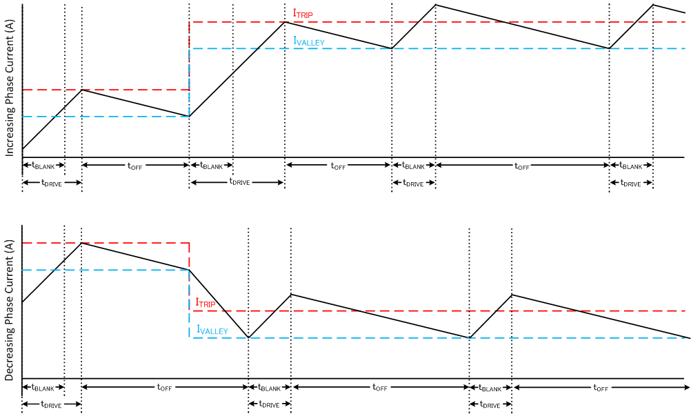
GUID-9E20B1C4-B248-4910-8811-9E5276103546-low.gifFigure 8-7 Smart tune Ripple Control Decay Mode

Smart tune Ripple Control operates by setting an IVALLEY level alongside the ITRIP level. When the current level reaches ITRIP, instead of entering slow decay until the tOFF time expires, the driver enters slow decay until IVALLEY is reached. Slow decay operates by turning on both low-side MOSFETs, allowing the current to recirculate. In this mode, tOFF varies depending on the current level and operating conditions.

The ripple current in this decay mode is 11 mA + 1% of ITRIP, where ITRIP is the regulation current of a particular microstep level.

The ripple control method allows much tighter regulation of the current level, thereby increasing motor efficiency and reducing audible noise and vibration. Smart tune Ripple Control can be used in systems that can tolerate a variable off-time regulation scheme to achieve small current ripple in the current regulation.