JAJSM96 may 2023 DRV8849
PRODUCTION DATA
- 1
- 1 特長
- 2 アプリケーション
- 3 概要
- 4 Revision History
- 5 Device Comparison
- 6 Pin Configuration and Functions
- 7 Specifications
-
8 Detailed Description
- 8.1 Overview
- 8.2 Functional Block Diagram
- 8.3 Feature Description
- 8.4 Device Functional Modes
- 9 Application and Implementation
- 10Layout
- 11デバイスおよびドキュメントのサポート
- 12Mechanical, Packaging, and Orderable Information
8.3.6 Logic Level, tri-level and quad-level Pin Diagrams
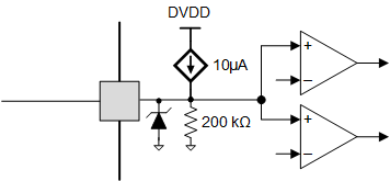
The following diagram shows the input structure for MODE0x, and ENABLE pins.
 Figure 8-10 Tri-Level Input Pin Diagram
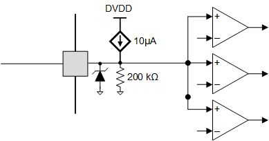
Figure 8-11 shows the input structure for MODE1x and DECAYx pins.
 Figure 8-11 Quad-Level Input Pin Diagram
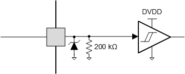
Figure 8-12 shows the input structure for STEP, DIR and nSLEEP pins.
 Figure 8-12 Logic-Level Input Pin Diagram