SNLS432C October 2012 – December 2015 DS125MB203
PRODUCTION DATA.
- 1 Features
- 2 Applications
- 3 Description
- 4 Revision History
- 5 Description continued
- 6 Pin Configuration and Functions
- 7 Specifications
- 8 Detailed Description
- 9 Application and Implementation
- 10Power Supply Recommendations
- 11Layout
- 12Device and Documentation Support
- 13Mechanical, Packaging, and Orderable Information
9 Application and Implementation
NOTE
Information in the following applications sections is not part of the TI component specification, and TI does not warrant its accuracy or completeness. TI’s customers are responsible for determining suitability of components for their purposes. Customers should validate and test their design implementation to confirm system functionality.
9.1 Application Information
9.1.1 General Recommendations
The DS125MB203 is a high-performance circuit capable of delivering excellent performance. Pay careful attention to the details associated with high-speed design as well as providing a clean power supply. Refer to the information below and Revision 4 of the LVDS Owner's Manual for more detailed information on high speed design tips to address signal integrity design issues.
 Figure 8. Test Set-Up Connections Diagram
 Figure 9. Test Set-Up Connections Diagram
9.2 Typical Application
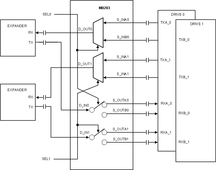
 Figure 10. Storage Application
9.2.1 Design Requirements
As with any high-speed design, there are many factors which influence the overall performance. Below are a list of critical areas for consideration and study during design:
- Use 100-Ω impedance traces. Generally these are very loosely coupled to ease routing length differences.
- Place AC-coupling capacitors near to the receiver end of each channel segment to minimize reflections.
- The maximum body size for AC-coupling capacitors is 0402.
- Back-drill connector vias and signal vias to minimize stub length.
- Use Reference plane vias to ensure a low inductance path for the return current.
9.2.2 Detailed Design Procedure
The DS125MB203 is designed to be placed at an offset location with respect to the overall channel attenuation. To optimize performance, the repeater requires tuning to extend the reach of the cable or trace length while also recovering a solid eye opening. To tune the mux-buffer, the settings mentioned in Table 2 and Table 3 are recommended as a default starting point for most applications. Once these settings are configured, additional tuning of the EQ and, to a lesser extent, VOD may be required to optimize the repeater performance for each specific application environment.
Examples of the repeater performance as a generic high-speed datapath repeater are shown in the performance curves in the Application Curves section.
9.2.3 Application Curves
![DS125MB203 TL = 10-inch 5–mil FR4
Trace, 8 Gbps
MB203 Settings: EQ[1:0] = 0, F = 02'h, DEM[1:0] = 0, 1 DS125MB203 30185459.png](/ods/images/SNLS432C/30185459.png) Figure 11. TL = 10-inch 5–mil FR4 Trace, 8 Gbps
Figure 11. TL = 10-inch 5–mil FR4 Trace, 8 GbpsMB203 Settings: EQ[1:0] = 0, F = 02'h, DEM[1:0] = 0, 1
![DS125MB203 TL = 30-inch 5–mil FR4
Trace, 8 Gbps
MB203 Settings: EQ[1:0] = R, 0 = 07'h, DEM[1:0] = 0, 1 DS125MB203 30185467.png](/ods/images/SNLS432C/30185467.png) Figure 13. TL = 30-inch 5–mil FR4 Trace, 8 Gbps
Figure 13. TL = 30-inch 5–mil FR4 Trace, 8 GbpsMB203 Settings: EQ[1:0] = R, 0 = 07'h, DEM[1:0] = 0, 1
![DS125MB203 TL = 20-inch 5–mil FR4
Trace, 8 Gbps
MB203 Settings: EQ[1:0] = 0, 1 = 03'h, DEM[1:0] = 0, 1 DS125MB203 30185461.png](/ods/images/SNLS432C/30185461.png) Figure 12. TL = 20-inch 5–mil FR4 Trace, 8 Gbps
Figure 12. TL = 20-inch 5–mil FR4 Trace, 8 GbpsMB203 Settings: EQ[1:0] = 0, 1 = 03'h, DEM[1:0] = 0, 1
![DS125MB203 TL1 = 20-inch 5–mil
FR4 Trace, TL2 = 10-inch 5–mil FR4 Trace, 8 Gbps
MB203 Settings: EQ[1:0] = R, 1 = 03'h, DEM[1:0] = R, 0 DS125MB203 30185463.png](/ods/images/SNLS432C/30185463.png) Figure 14. TL1 = 20-inch 5–mil FR4 Trace, TL2 = 10-inch 5–mil FR4 Trace, 8 Gbps
Figure 14. TL1 = 20-inch 5–mil FR4 Trace, TL2 = 10-inch 5–mil FR4 Trace, 8 GbpsMB203 Settings: EQ[1:0] = R, 1 = 03'h, DEM[1:0] = R, 0