JAJSI41B February   2017  – October 2019 DS250DF210

PRODUCTION DATA.  

  1. 特長
  2. アプリケーション
  3. 概要
    1.     Device Images
      1.      概略回路図
  4. 改訂履歴
  5. 概要(続き)
  6. Pin Configuration and Functions
    1.     Pin Functions
  7. Specifications
    1. 7.1  Absolute Maximum Ratings
    2. 7.2  ESD Ratings
    3. 7.3  Recommended Operating Conditions
    4. 7.4  Thermal Information
    5. 7.5  Electrical Characteristics
    6. 7.6  Timing Requirements, Retimer Jitter Specifications
    7. 7.7  Timing Requirements, Retimer Specifications
    8. 7.8  Timing Requirements, Recommended Calibration Clock Specifications
    9. 7.9  Recommended SMBus Switching Characteristics (Slave Mode)
    10. 7.10 Recommended SMBus Switching Characteristics (Master Mode)
    11. 7.11 Typical Characteristics
  8. Detailed Description
    1. 8.1 Overview
    2. 8.2 Functional Block Diagram
    3. 8.3 Feature Description
      1. 8.3.1  Device Data Path Operation
      2. 8.3.2  Signal Detect
      3. 8.3.3  Continuous Time Linear Equalizer (CTLE)
      4. 8.3.4  Variable Gain Amplifier (VGA)
      5. 8.3.5  Cross-Point Switch
      6. 8.3.6  Decision Feedback Equalizer (DFE)
      7. 8.3.7  Clock and Data Recovery (CDR)
      8. 8.3.8  Calibration Clock
      9. 8.3.9  Differential Driver With FIR Filter
        1. 8.3.9.1 Setting the Output VOD, Precursor, and Postcursor Equalization
        2. 8.3.9.2 Output Driver Polarity Inversion
      10. 8.3.10 Debug Features
        1. 8.3.10.1 Pattern Generator
        2. 8.3.10.2 Pattern Checker
        3. 8.3.10.3 Eye Opening Monitor
      11. 8.3.11 Interrupt Signals
    4. 8.4 Device Functional Modes
      1. 8.4.1 Supported Data Rates
      2. 8.4.2 SMBus Master Mode
      3. 8.4.3 Device SMBus Address
    5. 8.5 Programming
      1. 8.5.1 Bit Fields in the Register Set
      2. 8.5.2 Writing to and Reading from the Global/Shared/Channel Registers
    6. 8.6 Register Maps
  9. Application and Implementation
    1. 9.1 Application Information
    2. 9.2 Typical Applications
      1. 9.2.1 Front-Port Jitter Cleaning Applications
        1. 9.2.1.1 Design Requirements
        2. 9.2.1.2 Detailed Design Procedure
      2. 9.2.2 Active Cable Applications
        1. 9.2.2.1 Design Requirements
        2. 9.2.2.2 Detailed Design Procedure
      3. 9.2.3 Backplane and Mid-Plane Applications
      4. 9.2.4 Design Requirements
      5. 9.2.5 Detailed Design Procedure
      6. 9.2.6 Application Curves
  10. 10Power Supply Recommendations
  11. 11Layout
    1. 11.1 Layout Guidelines
    2. 11.2 Layout Example
  12. 12デバイスおよびドキュメントのサポート
    1. 12.1 デバイス・サポート
      1. 12.1.1 開発サポート
    2. 12.2 ドキュメントのサポート
      1. 12.2.1 関連資料
    3. 12.3 ドキュメントの更新通知を受け取る方法
    4. 12.4 サポート・リソース
    5. 12.5 商標
    6. 12.6 静電気放電に関する注意事項
    7. 12.7 Glossary
  13. 13メカニカル、パッケージ、および注文情報

パッケージ・オプション

メカニカル・データ(パッケージ|ピン)
サーマルパッド・メカニカル・データ
発注情報

Typical Characteristics

DS250DF210 C001_SNLS495_VOD_vs_VDD.pngFigure 1. Typical VOD vs Supply Voltage
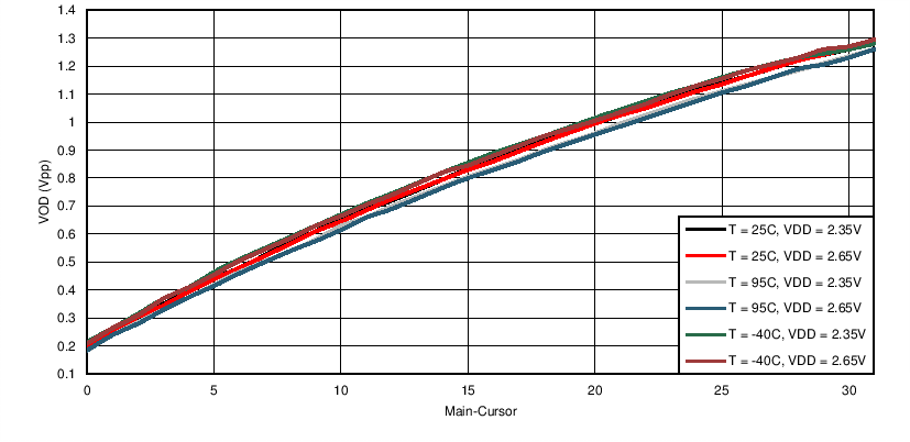
DS250DF210 VOD_vs_Main_SNLS513.png
Figure 3. Typical VOD vs FIR Main-Cursor
DS250DF210 IJT_allfreq_SNLS513.png
0.1 MHz to 100 MHz Input Random Jitter = 0.078 UIpp
T = 25°C
Figure 5. Typical Sinusoidal Input Jitter Tolerance for
30-dB Channel at 25.78125 Gbps
DS250DF210 C002_SNLS495_VOD_vs_Temp.pngFigure 2. Typical VOD vs Temperature
DS250DF210 jitter_vs_temp_SNLS513.png
Figure 4. Typical Output Jitter vs Temperature
at 25.78125 Gbps
DS250DF210 IJT_higherfreq_SNLS513.png
0.5 MHz to 100 MHz Input Random Jitter = 0.078 UIpp
T = 25°C
Figure 6. Typical Input Jitter Tolerance for
300-dB Channel at 25.78125 Gbps