JAJSI43C December 2015 – October 2019 DS250DF810
PRODUCTION DATA.
- 1 特長
- 2 アプリケーション
- 3 概要
- 4 改訂履歴
- 5 概要(続き)
- 6 Pin Configuration and Functions
-
7 Specifications
- 7.1 Absolute Maximum Ratings
- 7.2 ESD Ratings
- 7.3 Recommended Operating Conditions
- 7.4 Thermal Information
- 7.5 Electrical Characteristics
- 7.6 Timing Requirements, Retimer Jitter Specifications
- 7.7 Timing Requirements, Retimer Specifications
- 7.8 Timing Requirements, Recommended Calibration Clock Specifications
- 7.9 Recommended SMBus Switching Characteristics (Slave Mode)
- 7.10 Recommended SMBus Switching Characteristics (Master Mode)
- 7.11 Typical Characteristics
-
8 Detailed Description
- 8.1 Overview
- 8.2 Functional Block Diagram
- 8.3
Feature Description
- 8.3.1 Device Data Path Operation
- 8.3.2 AC-Coupled Receiver and Transmitter
- 8.3.3 Signal Detect
- 8.3.4 Continuous Time Linear Equalizer (CTLE)
- 8.3.5 Variable Gain Amplifier (VGA)
- 8.3.6 Cross-Point Switch
- 8.3.7 Decision Feedback Equalizer (DFE)
- 8.3.8 Clock and Data Recovery (CDR)
- 8.3.9 Calibration Clock
- 8.3.10 Differential Driver with FIR Filter
- 8.3.11 Setting the Output VOD
- 8.3.12 Output Driver Polarity Inversion
- 8.3.13 Debug Features
- 8.3.14 Interrupt Signals
- 8.4 Device Functional Modes
- 8.5 Programming
- 8.6 Register Maps
- 9 Application and Implementation
- 10Power Supply Recommendations
- 11Layout
- 12デバイスおよびドキュメントのサポート
- 13メカニカル、パッケージ、および注文情報
7.11 Typical Characteristics
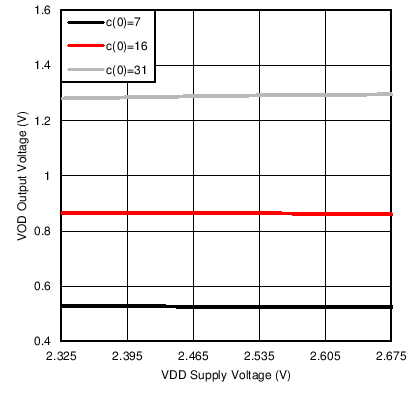 Figure 1. Typical VOD versus Supply Voltage
 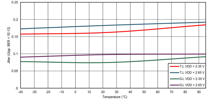 Figure 3. Typical VOD versus FIR Main-Cursor
 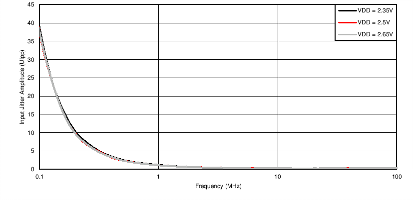 Figure 5. Typical Sinusoidal Input Jitter Tolerance for 30dB channel at 25.78125Gbps for 0.1MHz to 100MHz with Input Random Jitter = 0.078UIpp, T = 25C
 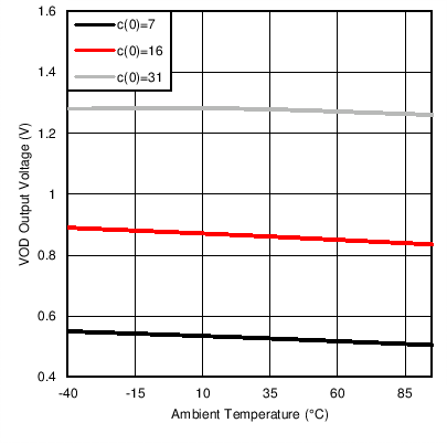 Figure 2. Typical VOD versus Temperature
 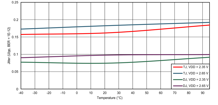 Figure 4. Typical Output Jitter versus Temperature at 25.78125Gbps
 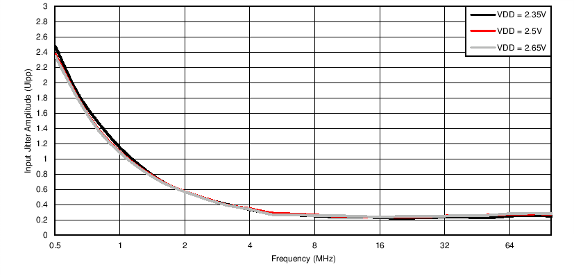 Figure 6. Typical Input Jitter Tolerance for 30dB channel at 25.78125Gbps for 0.5MHz to 100MHz with Input Random Jitter = 0.078UIpp, T = 25C