JAJSI57B September 2016 – February 2024 DS280DF810
PRODUCTION DATA
- 1
- 1 特長
- 2 アプリケーション
- 3 概要
- 4 Pin Configuration and Functions
-
5 Specifications
- 5.1 Absolute Maximum Ratings
- 5.2 ESD Ratings
- 5.3 Recommended Operating Conditions
- 5.4 Thermal Information
- 5.5 Electrical Characteristics
- 5.6 Timing Requirements, Retimer Jitter Specifications
- 5.7 Timing Requirements, Retimer Specifications
- 5.8 Timing Requirements, Recommended Calibration Clock Specifications
- 5.9 Recommended SMBus Switching Characteristics (Target Mode)
- 5.10 Recommended SMBus Switching Characteristics (Controller Mode)
- 5.11 Typical Characteristics
-
6 Detailed Description
- 6.1 Overview
- 6.2 Functional Block Diagram
- 6.3
Feature Description
- 6.3.1
Device Data Path Operation
- 6.3.1.1 AC-Coupled Receiver and Transmitter
- 6.3.1.2 Signal Detect
- 6.3.1.3 Continuous Time Linear Equalizer (CTLE)
- 6.3.1.4 Variable Gain Amplifier (VGA)
- 6.3.1.5 2x2 Cross-Point Switch
- 6.3.1.6 Decision Feedback Equalizer (DFE)
- 6.3.1.7 Clock and Data Recovery (CDR)
- 6.3.1.8 Calibration Clock
- 6.3.1.9 Differential Driver with FIR Filter
- 6.3.2 Debug Features
- 6.3.1
Device Data Path Operation
- 6.4 Device Functional Modes
- 6.5 Programming
- 6.6 Register Maps
- 7 Application and Implementation
- 8 Device and Documentation Support
- 9 Revision History
- 10Mechanical, Packaging, and Orderable Information
パッケージ・オプション
デバイスごとのパッケージ図は、PDF版データシートをご参照ください。
メカニカル・データ(パッケージ|ピン)
- ABW|135
- ABV|135
サーマルパッド・メカニカル・データ
発注情報
6.3.1.5 2x2 Cross-Point Switch
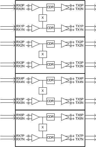
Between each group of two adjacent channels (for example, between channels 0–1, 2–3, 4–5, and 6–7) is a full 2×2 cross-point switch. The cross-point can be configured through SMBus registers to operate as follows:
- Straigh-thru mode
- Multiplex two inputs to one output
- Fanout one input to two outputs
- Cross two inputs to two outputs
Figure 6-1 shows the four 2x2 cross-points available in the DS280DF810, and Figure 6-2 shows how each cross-point can be configured for straight-thru, multiplex, de-multiplex, or cross-over applications. Refer to the DS280DF810 Programming Guide for details on how to program the cross-point through SMBus registers.
 Figure 6-1 Block
diagram showing all four 2x2 cross-points in the DS280DF810
 Figure 6-2 Signal
distribution options available in each 2x2 cross-point (channel A can be 0, 2,
4, or 6; channel B can be 1, 3, 5, or 7)