JAJS591D March 2000 – June 2016 DS90LV027A
PRODUCTION DATA.
6 Specifications
6.1 Absolute Maximum Ratings
over operating free-air temperature range (unless otherwise noted)(1)| MIN | MAX | UNIT | ||
|---|---|---|---|---|
| Supply voltage, VCC | –0.3 | 4 | V | |
| Input voltage, DI | –0.3 | 3.6 | V | |
| Output voltage, DO± | –0.3 | 3.9 | V | |
| Maximum package power dissipation at 25°C | D package | 1190 | mW | |
| Derate D package | 9.5 mW/°C above 25°C |
°C | ||
| Lead temperature range, soldering (4 s) | 260 | °C | ||
| Storage temperature, Tstg | –65 | 150 | °C | |
(1) Stresses beyond those listed under Absolute Maximum Ratings may cause permanent damage to the device. These are stress ratings only, which do not imply functional operation of the device at these or any other conditions beyond those indicated under Recommended Operating Conditions. Exposure to absolute-maximum-rated conditions for extended periods may affect device reliability.
6.2 ESD Ratings
| VALUE | UNIT | |||
|---|---|---|---|---|
| V(ESD) | Electrostatic discharge | Human-body model (HBM), per ANSI/ESDA/JEDEC JS-001(1) | ±8000 | V |
| Charged-device model (CDM), per JEDEC specification JESD22-C101(2) | ±1000 | |||
| EIAJ, 0 Ω, 200 pF | ±1000 | |||
| IEC direct, 330 Ω, 150 pF | ±4000 | |||
(1) JEDEC document JEP155 states that 500-V HBM allows safe manufacturing with a standard ESD control process.
(2) JEDEC document JEP157 states that 250-V CDM allows safe manufacturing with a standard ESD control process.
6.3 Recommended Operating Conditions
over operating free-air temperature range (unless otherwise noted)| MIN | NOM | MAX | UNIT | ||
|---|---|---|---|---|---|
| VCC | Supply voltage | 3 | 3.3 | 3.6 | V |
| TA | Operating free-air temperature | –40 | 25 | 85 | °C |
6.4 Thermal Information
| THERMAL METRIC(1) | DS90LV027A | UNIT | ||
|---|---|---|---|---|
| D (SOIC) | ||||
| 8 PINS | ||||
| RθJA | Junction-to-ambient thermal resistance | Low-K thermal resistance(2) | 212 | °C/W |
| High-K thermal resistance(2) | 112 | |||
| RθJC(top) | Junction-to-case (top) thermal resistance | 69.1 | °C/W | |
| RθJB | Junction-to-board thermal resistance | 47.7 | °C/W | |
| ψJT | Junction-to-top characterization parameter | 15.2 | °C/W | |
| ψJB | Junction-to-board characterization parameter | 47.2 | °C/W | |
| RθJC(bot) | Junction-to-case (bottom) thermal resistance | — | °C/W | |
(1) For more information about traditional and new thermal metrics, see the Semiconductor and IC Package Thermal Metrics application report.
(2) Tested in accordance with the Low-K or High-K thermal metric definitions of EIA/JESD51-3 for leaded surface-mount packages.
6.5 Electrical Characteristics
over operating free-air temperature range (unless otherwise noted)(1)(3)| PARAMETER | TEST CONDITIONS | MIN | TYP(2) | MAX | UNIT | |||
|---|---|---|---|---|---|---|---|---|
| VOD | Output differential voltage | RL = 100 Ω (see Figure 15), DO+, DO− pins | 250 | 360 | 450 | mV | ||
| ΔVOD | VOD magnitude change | RL = 100 Ω (see Figure 15), DO+, DO− pins | 1 | 35 | mV | |||
| VOH | Output high voltage | RL = 100 Ω (see Figure 15), DO+, DO− pins | 1.4 | 1.6 | V | |||
| VOL | Output low voltage | RL = 100 Ω (see Figure 15), DO+, DO− pins | 0.9 | 1.1 | V | |||
| VOS | Offset voltage | RL = 100 Ω (see Figure 15), DO+, DO− pins | 1.125 | 1.2 | 1.375 | V | ||
| ΔVOS | Offset magnitude change | RL = 100 Ω (see Figure 15), DO+, DO− pins | 0 | 3 | 25 | mV | ||
| IOXD | Power-off leakage | VOUT = VCC or GND, VCC = 0 V, DO+, DO− pins | ±1 | ±10 | μA | |||
| IOSD | Output short-circuit current | DO+, DO− pins | –5.7 | –8 | mA | |||
| VIH | Input high voltage | DI pin | 2 | VCC | V | |||
| VIL | Input low voltage | DI pin | GND | 0.8 | V | |||
| IIH | Input high current | VIN = 3.3 V or 2.4 V, DI pin | ±2 | ±10 | μA | |||
| IIL | Input low current | VIN = GND or 0.5 V, DI pin | ±1 | ±10 | μA | |||
| VCL | Input clamp voltage | ICL = −18 mA, DI pin | –1.5 | –0.6 | V | |||
| ICC | Power supply current | VIN = VCC or GND, VCC pin | No load | 8 | 14 | mA | ||
| RL = 100 Ω | 14 | 20 | ||||||
(1) Current into device pins is defined as positive. Current out of device pins is defined as negative. All voltages are referenced to ground except VOD.
(2) All typicals are given for: VCC = 3.3 V and TA = 25°C.
(3) The DS90LV027A is a current mode device and only function with datasheet specification when a resistive load is applied to the drivers outputs.
6.6 Switching Characteristics
RL = 100 Ω and CL = 15 pF, see Figure 16 and Figure 17 (unless otherwise noted)(1)(2)(3)| PARAMETER | TEST CONDITIONS | MIN | TYP(4) | MAX | UNIT | |
|---|---|---|---|---|---|---|
| tPHLD | Differential propagation delay high to low | 0.3 | 0.8 | 1.5 | ns | |
| tPLHD | Differential propagation delay low to high | 0.3 | 1.1 | 1.5 | ns | |
| tSKD1 | Differential pulse skew |tPHLD − tPLHD|(5) | 0 | 0.3 | 0.7 | ns | |
| tSKD2 | Channel to channel skew(6) | 0 | 0.4 | 0.8 | ns | |
| tSKD3 | Differential part to part skew(7) | 0 | 1 | ns | ||
| tSKD4 | Differential part to part skew(8) | 0 | 1.2 | ns | ||
| tTLH | Transition low to high time | 0.2 | 0.5 | 1 | ns | |
| tTHL | Transition high to low time | 0.2 | 0.5 | 1 | ns | |
| fMAX | Maximum operating frequency(9) | 350 | MHz | |||
(1) These parameters are ensured by design. The limits are based on statistical analysis of the device over PVT (process, voltage, temperature) ranges.
(2) CL includes probe and fixture capacitance.
(3) Generator waveform for all tests unless otherwise specified: f = 1 MHz, ZO = 50 Ω, tr ≤ 1 ns, tf ≤ 1 ns (10%-90%).
(4) All typicals are given for: VCC = 3.3 V and TA = 25°C.
(5) tSKD1, |tPHLD − tPLHD|, is the magnitude difference in differential propagation delay time between the positive going edge and the negative going edge of the same channel.
(6) tSKD2 is the Differential Channel to Channel Skew of any event on the same device.
(7) tSKD3, Differential Part to Part Skew, is defined as the difference between the minimum and maximum specified differential propagation delays. This specification applies to devices at the same VCC and within 5°C of each other within the operating temperature range.
(8) tSKD4, part to part skew, is the differential channel to channel skew of any event between devices. This specification applies to devices over recommended operating temperature and voltage ranges, and across process distribution. tSKD4 is defined as |Max − Min| differential propagation delay.
(9) fMAX generator input conditions: tr = tf < 1 ns (0% to 100%), 50% duty cycle, 0 V to 3 V. Output criteria: duty cycle = 45% / 55%,
VOD > 250 mV, all channels switching.
VOD > 250 mV, all channels switching.
6.7 Typical Characteristics
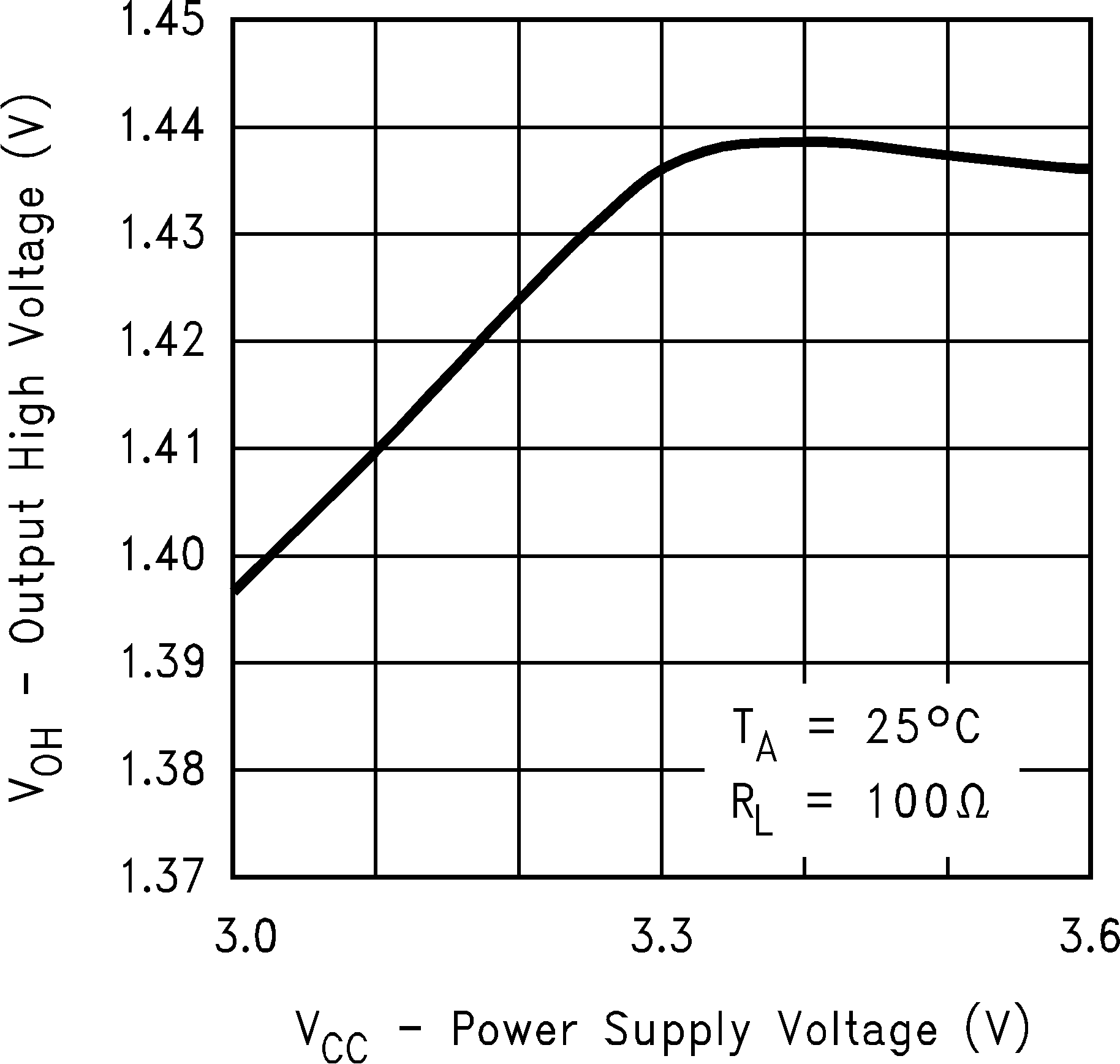 Figure 1. Output High Voltage
 vs Power Supply Voltage
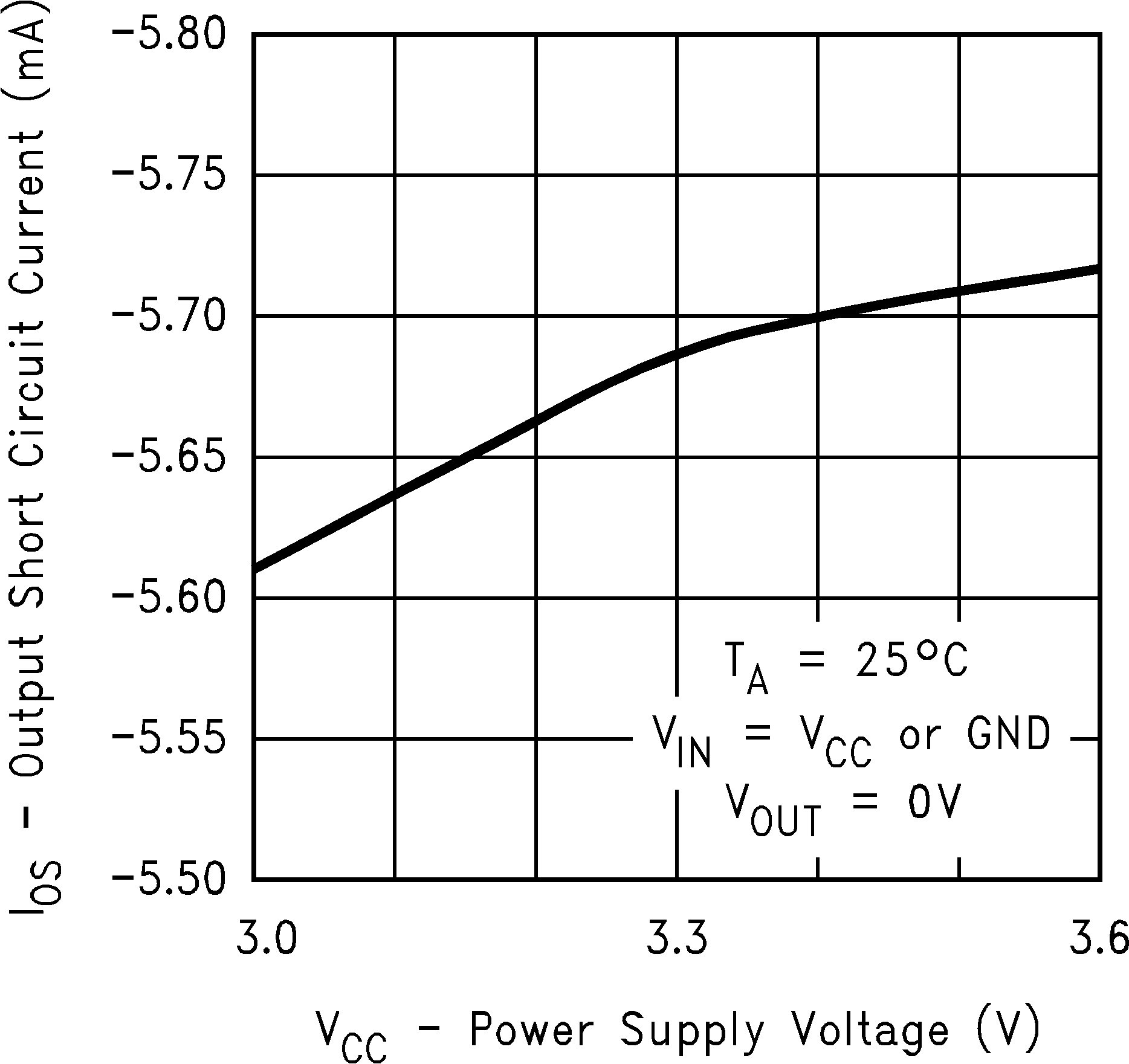 Figure 3. Output Short-Circuit Current
 vs Power Supply Voltage
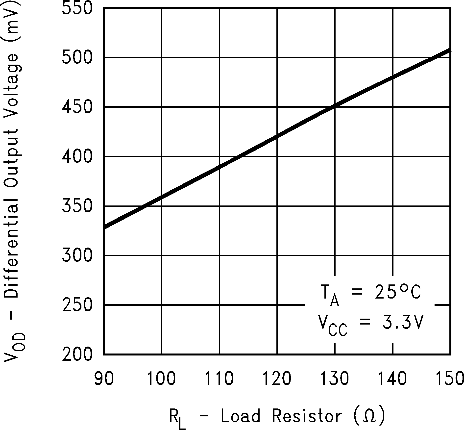 Figure 5. Differential Output Voltage
 vs Load Resistor
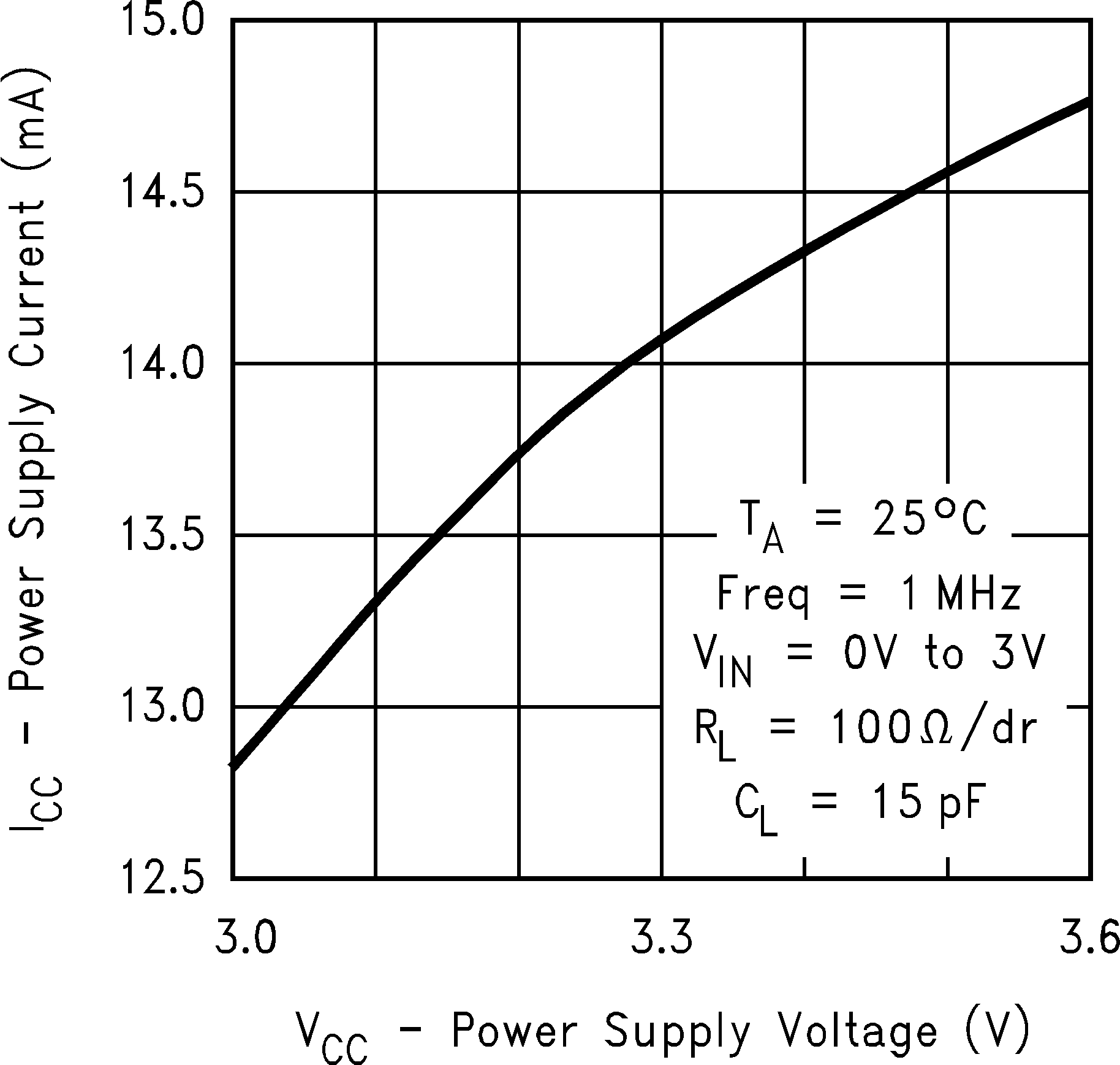 Figure 7. Power Supply Current
 vs Power Supply Voltage
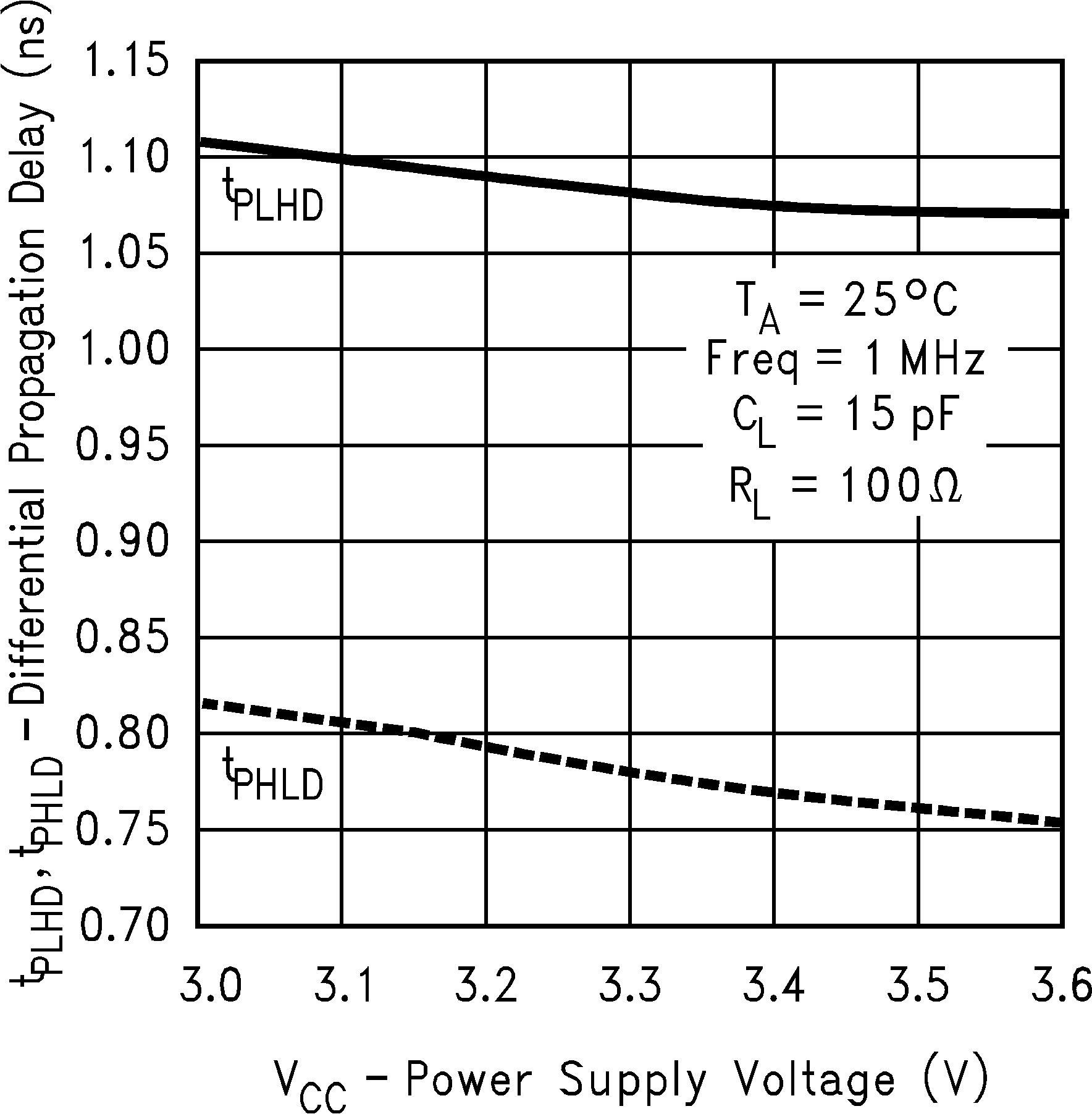 Figure 9. Differential Propagation Delay
 vs Power Supply Voltage
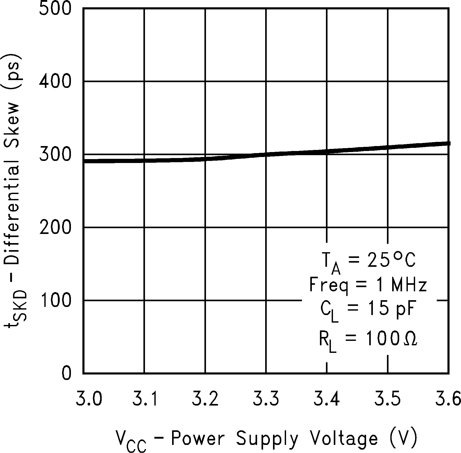 Figure 11. Differential Skew
 vs Power Supply Voltage
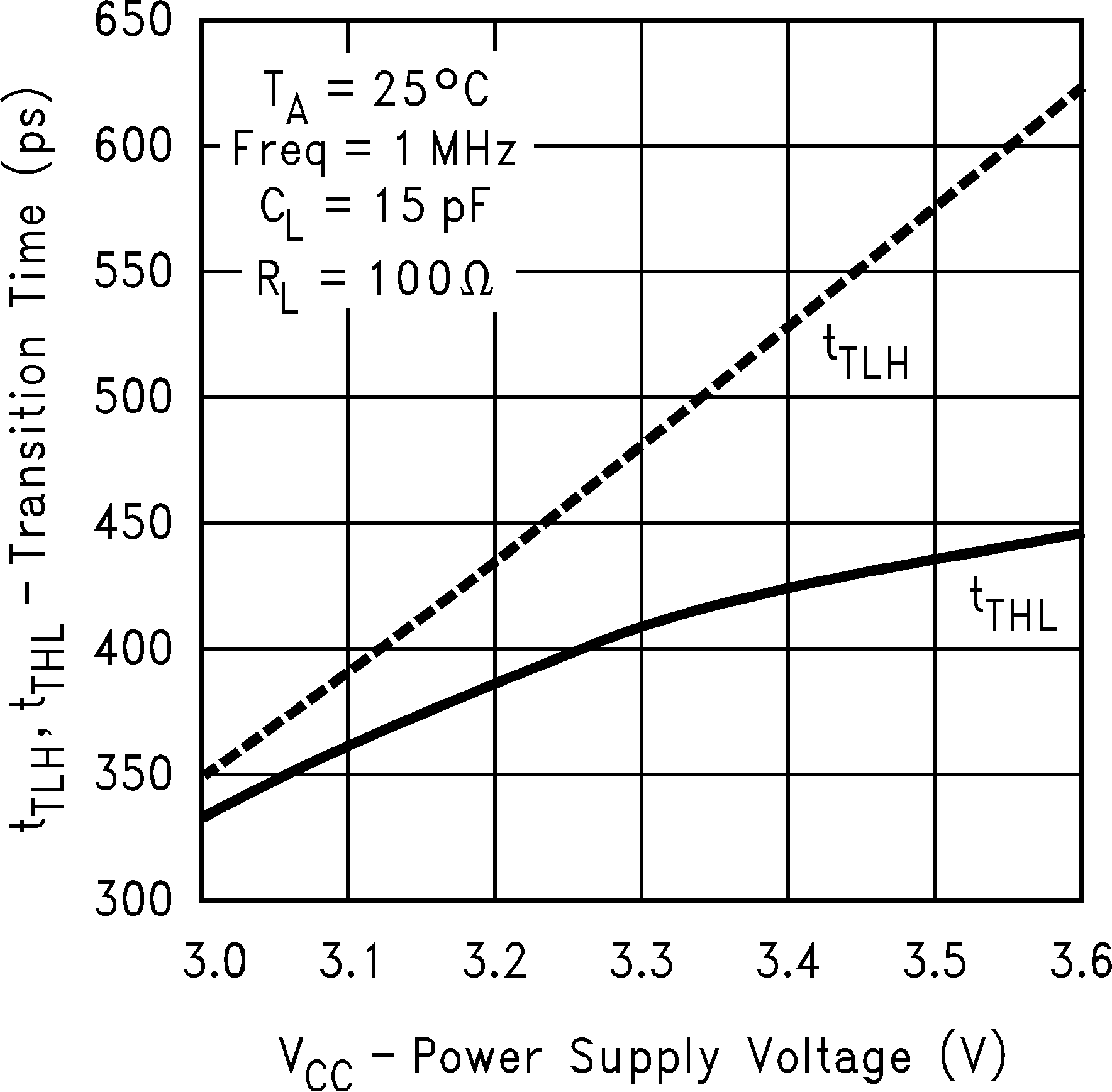 Figure 13. Transition Time
 vs Power Supply Voltage
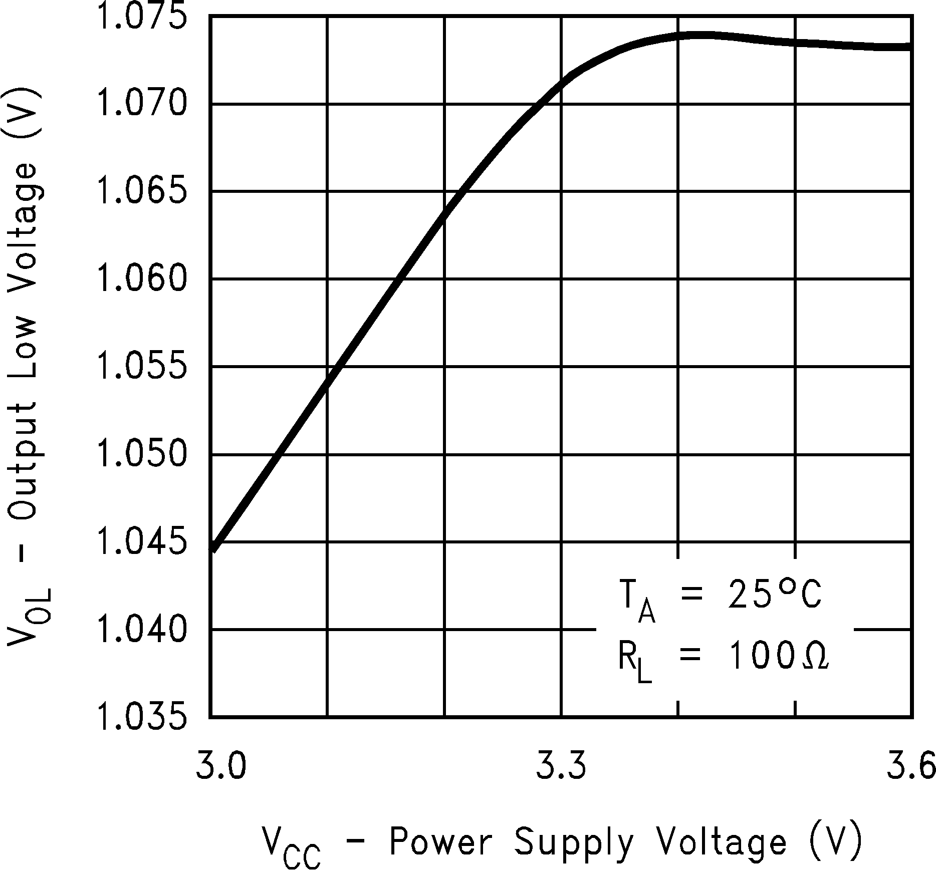 Figure 2. Output Low Voltage
 vs Power Supply Voltage
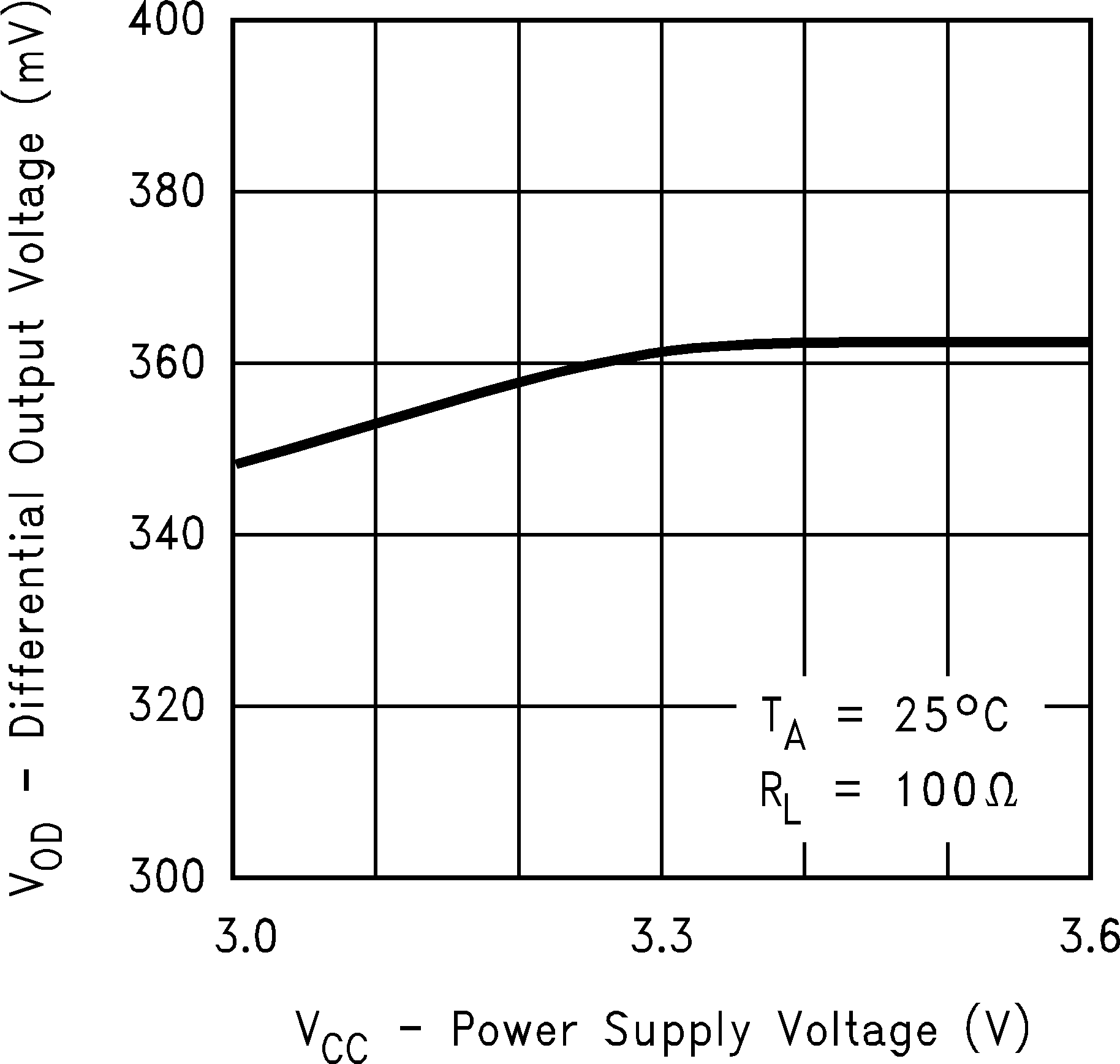 Figure 4. Differential Output Voltage
 vs Power Supply Voltage
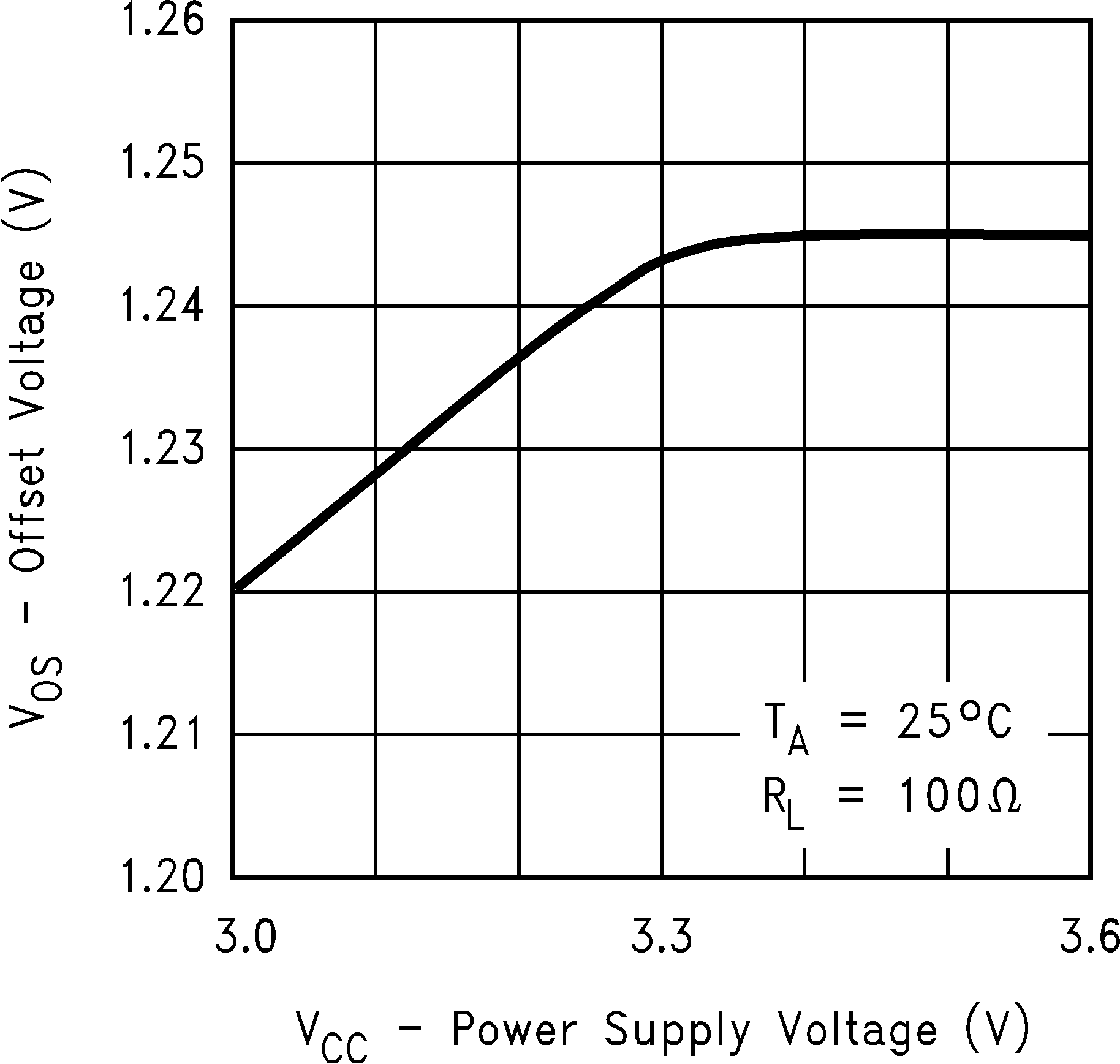 Figure 6. Offset Voltage
 vs Power Supply Voltage
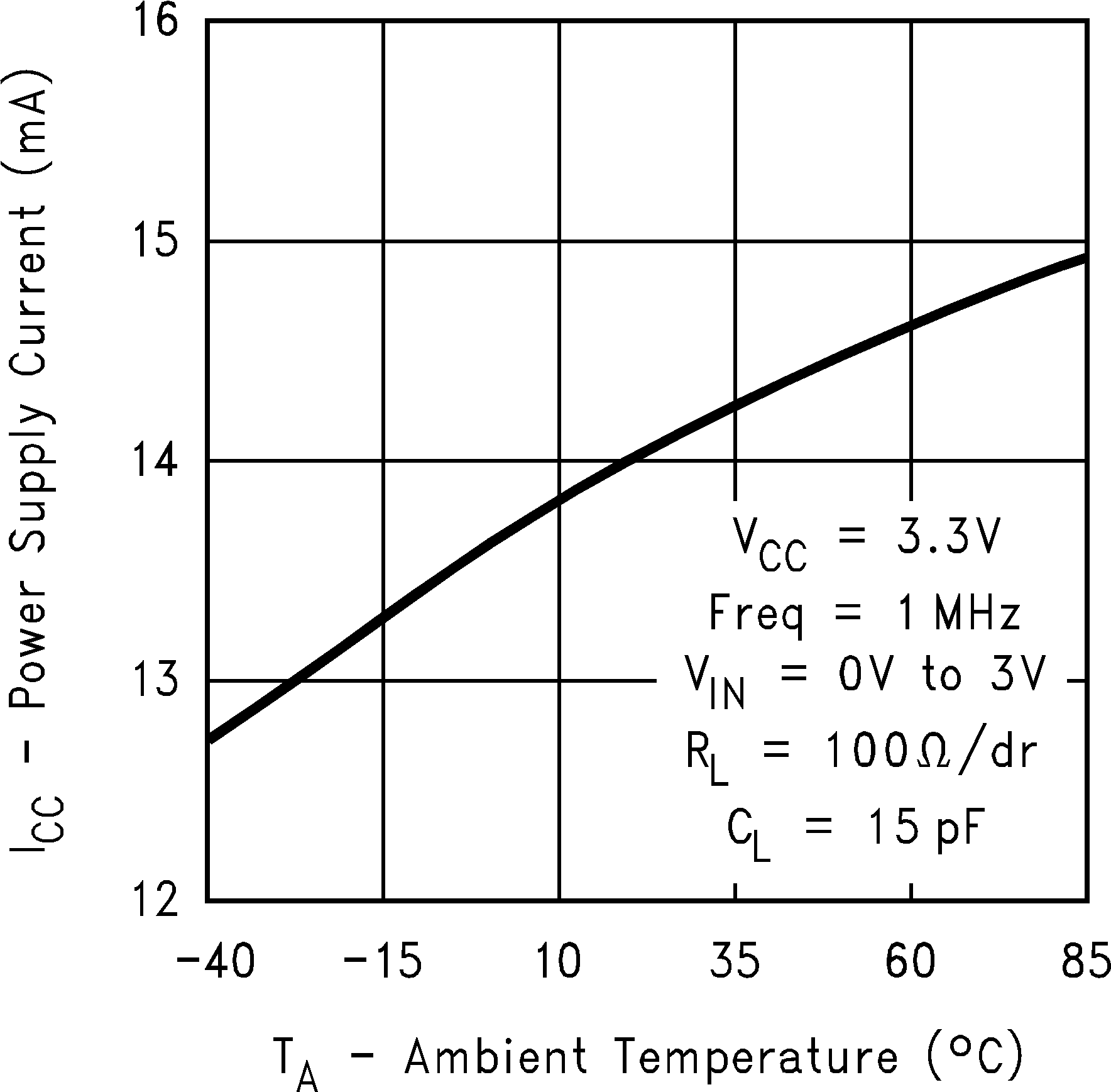 Figure 8. Power Supply Current
 vs Ambient Temperature
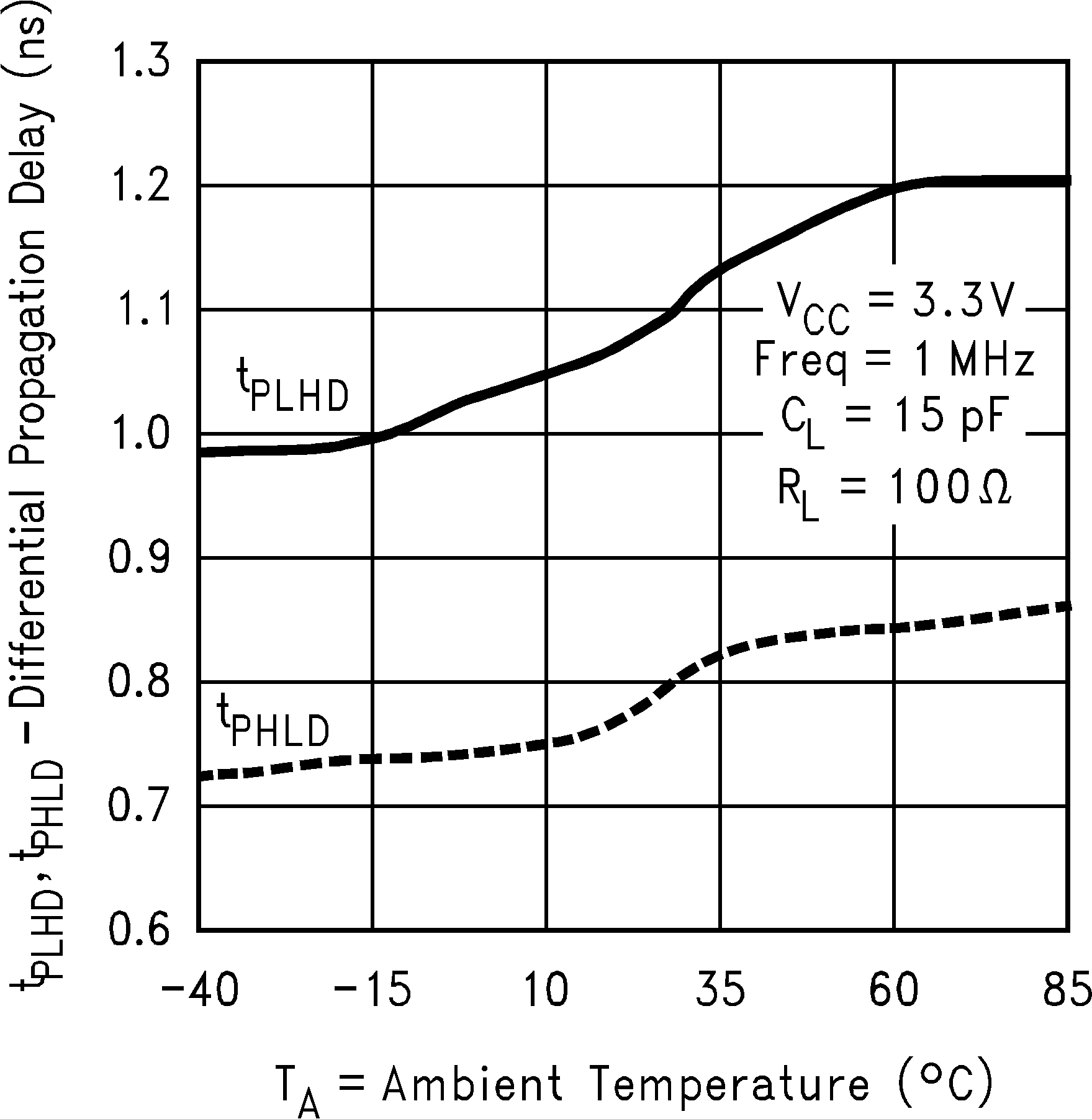 Figure 10. Differential Propagation Delay
 vs Ambient Temperature
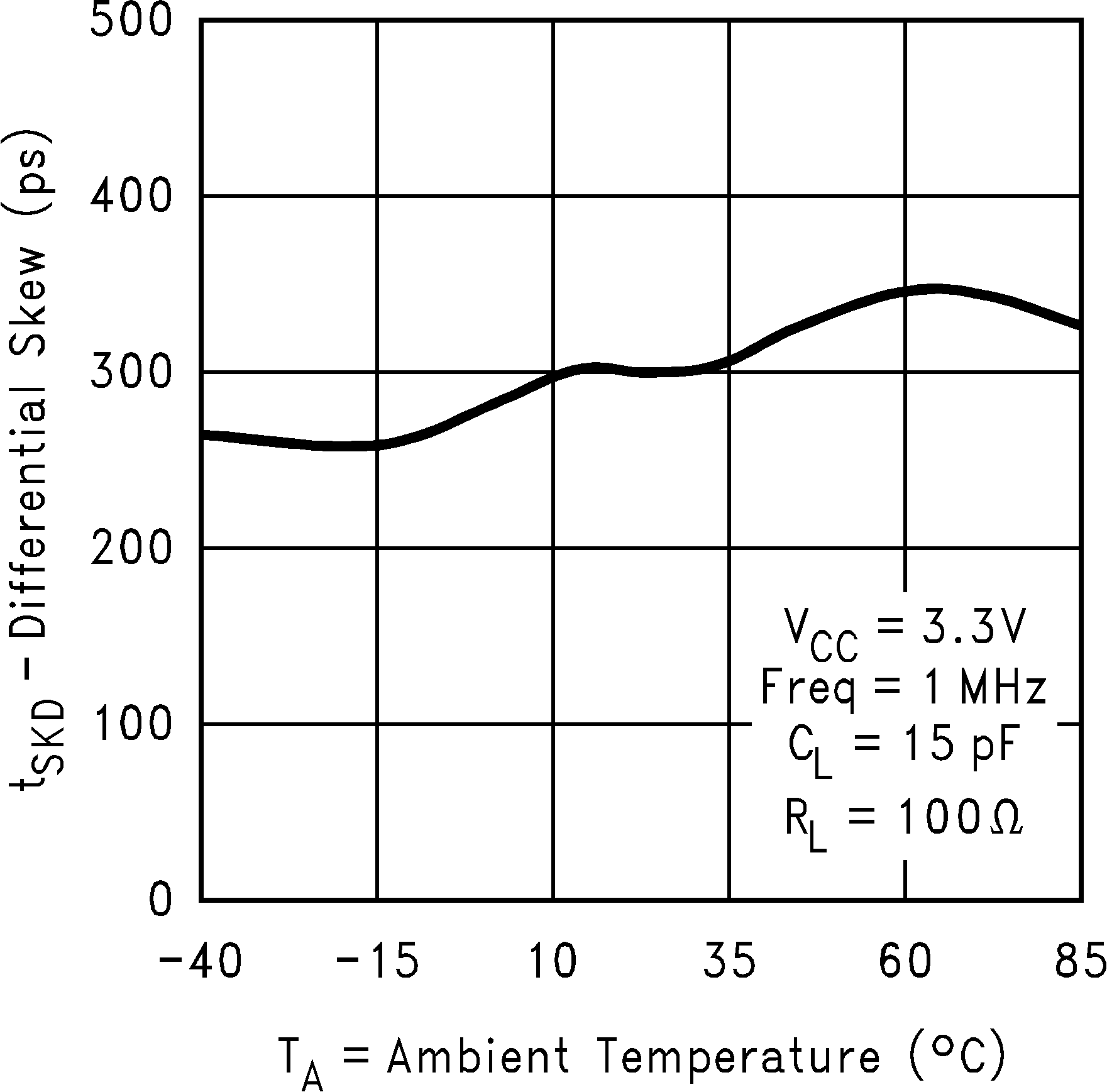 Figure 12. Differential Skew
 vs Ambient Temperature
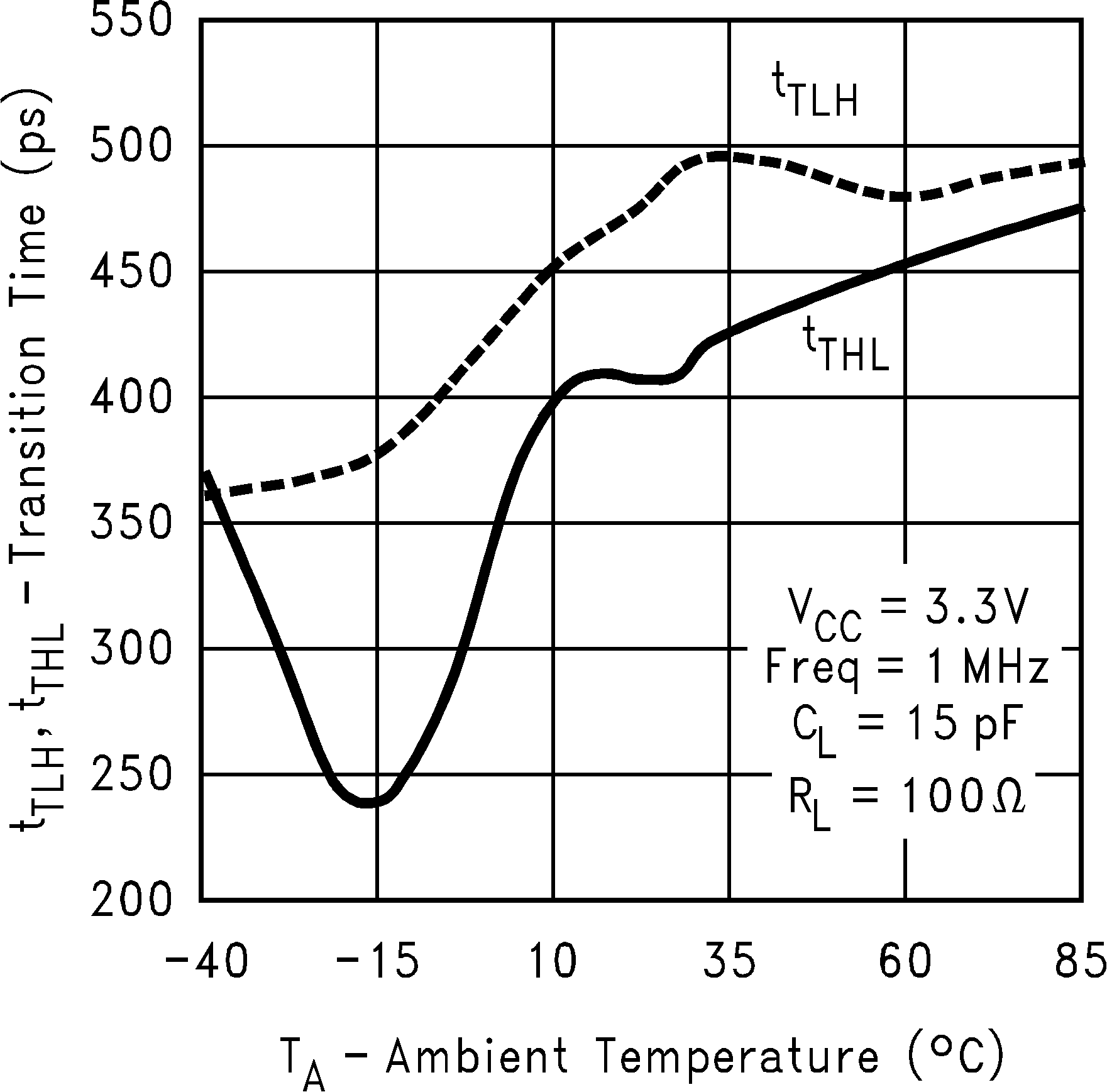 Figure 14. Transition Time
 vs Ambient Temperature