JAJSGU7B September 2005 – January 2019 DS90LV027AH
PRODUCTION DATA.
- 1 特長
- 2 アプリケーション
- 3 概要
- 4 改訂履歴
- 5 Pin Configuration and Functions
- 6 Specifications
- 7 Parameter Measurement Information
- 8 Detailed Description
- 9 Application and Implementation
- 10Power Supply Recommendations
- 11Layout
- 12デバイスおよびドキュメントのサポート
- 13メカニカル、パッケージ、および注文情報
9.2.2.6 PCB Transmission Lines
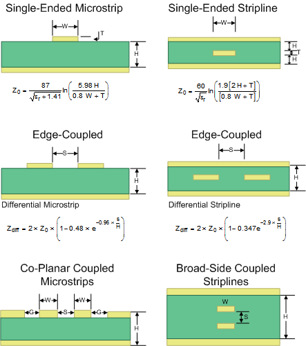
As per the LVDS Owner's Manual Design Guide, 4th Edition (SNLA187), Figure 22 depicts several transmission line structures commonly used in printed-circuit boards (PCBs). Each structure consists of a signal line and return path with a uniform cross section along its length. A microstrip is a signal trace on the top (or bottom) layer, separated by a dielectric layer from its return path in a ground or power plane. A stripline is a signal trace in the inner layer, with a dielectric layer in between a ground plane above and below the signal trace. The dimensions of the structure along with the dielectric material properties determine the characteristic impedance of the transmission line (also called controlled-impedance transmission line).
When two signal lines are placed close by, they form a pair of coupled transmission lines. Figure 22 shows examples of edge-coupled microstrip lines, and edge-coupled or broad-side-coupled striplines. When excited by differential signals, the coupled transmission line is referred to as a differential pair. The characteristic impedance of each line is called odd-mode impedance. The sum of the odd-mode impedances of each line is the differential impedance of the differential pair. In addition to the trace dimensions and dielectric material properties, the spacing between the two traces determines the mutual coupling and impacts the differential impedance. When the two lines are immediately adjacent (like if S is less than 2 W, for example), the differential pair is called a tightly-coupled differential pair. To maintain constant differential impedance along the length, it is important to keep the trace width and spacing uniform along the length, as well as maintain good symmetry between the two lines.
 Figure 22. Controlled-Impedance Transmission Lines