JAJSGU7B September   2005  – January 2019 DS90LV027AH

PRODUCTION DATA.  

  1. 特長
  2. アプリケーション
  3. 概要
    1.     Device Images
      1.      チャネル 1 の機能図
      2.      チャネル 2 の機能図
  4. 改訂履歴
  5. Pin Configuration and Functions
    1.     Pin Functions
  6. Specifications
    1. 6.1 Absolute Maximum Ratings
    2. 6.2 ESD Ratings
    3. 6.3 Recommended Operating Conditions
    4. 6.4 Thermal Information
    5. 6.5 Electrical Characteristics
    6. 6.6 Switching Characteristics
    7. 6.7 Typical Characteristics
  7. Parameter Measurement Information
  8. Detailed Description
    1. 8.1 Overview
    2. 8.2 Functional Block Diagrams
    3. 8.3 Feature Description
      1. 8.3.1 DS90LV027AH Driver Functionality
      2. 8.3.2 Driver Output Voltage and Power-On Reset
      3. 8.3.3 Driver Offset
    4. 8.4 Device Functional Modes
  9. Application and Implementation
    1. 9.1 Application Information
    2. 9.2 Typical Application
      1. 9.2.1 Design Requirements
      2. 9.2.2 Detailed Design Procedure
        1. 9.2.2.1 Driver Supply Voltage
        2. 9.2.2.2 Driver Bypass Capacitance
        3. 9.2.2.3 Driver Input Votlage
        4. 9.2.2.4 Driver Output Voltage
        5. 9.2.2.5 Interconnecting Media
        6. 9.2.2.6 PCB Transmission Lines
      3. 9.2.3 Termination Resistor
      4. 9.2.4 Application Curve
  10. 10Power Supply Recommendations
  11. 11Layout
    1. 11.1 Layout Guidelines
      1. 11.1.1 Microstrip vs. Stripline Topologies
      2. 11.1.2 Dielectric Type and Board Construction
      3. 11.1.3 Recommended Stack Layout
      4. 11.1.4 Separation Between Traces
      5. 11.1.5 Crosstalk and Ground Bounce Minimization
      6. 11.1.6 Decoupling
    2. 11.2 Layout Example
  12. 12デバイスおよびドキュメントのサポート
    1. 12.1 関連資料
    2. 12.2 ドキュメントの更新通知を受け取る方法
    3. 12.3 コミュニティ・リソース
    4. 12.4 商標
    5. 12.5 静電気放電に関する注意事項
    6. 12.6 Glossary
  13. 13メカニカル、パッケージ、および注文情報

パッケージ・オプション

メカニカル・データ(パッケージ|ピン)
サーマルパッド・メカニカル・データ
発注情報

Microstrip vs. Stripline Topologies

As per the LVDS Application and Data Handbook (SLLD009), printed-circuit boards usually offer designers two transmission line options: Microstrip and stripline. Microstrips are traces on the outer layer of a PCB, as shown in Figure 24.
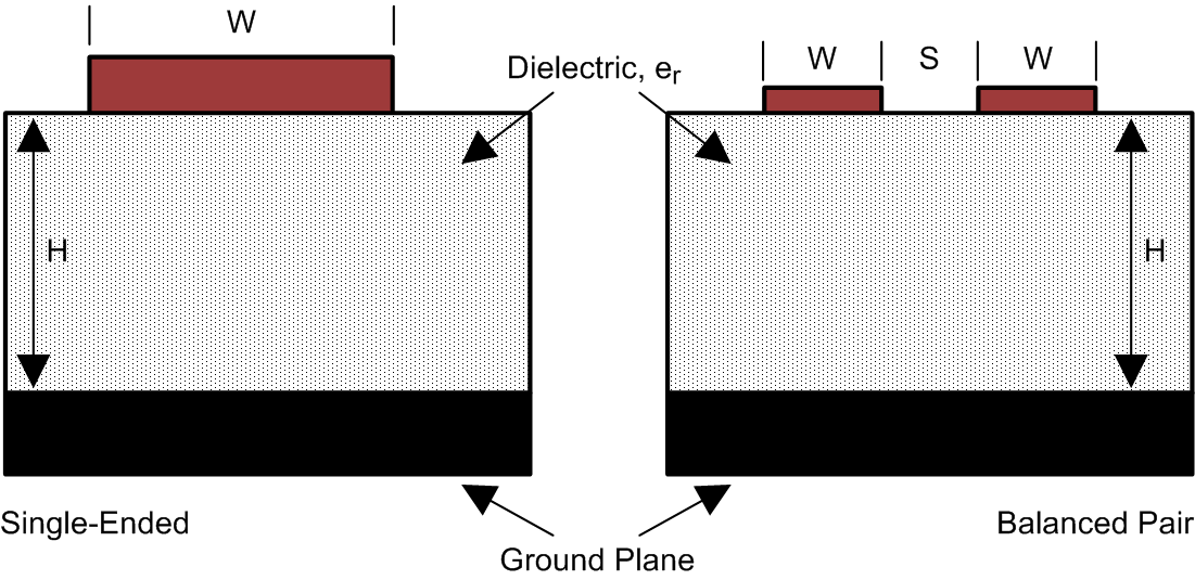
DS90LV027AH lo_mt_slls373.pngFigure 24. Microstrip Topology

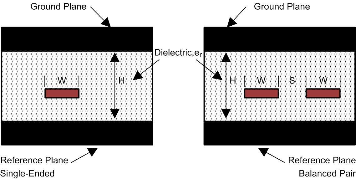
On the other hand, striplines are traces between two ground planes. Striplines are less prone to emissions and susceptibility problems because the reference planes effectively shield the embedded traces. However, from the standpoint of high-speed transmission, juxtaposing two planes creates additional capacitance. TI recommends routing LVDS signals on microstrip transmission lines when possible. The PCB traces allow designers to specify the necessary tolerances for ZO based on the overall noise budget and reflection allowances. Footnotes 1(2), 2(3), and 3(4) provide formulas for ZO and tPD for differential and single-ended traces. (2)(3)(4)
Howard Johnson & Martin Graham.1993. High Speed Digital Design – A Handbook of Black Magic. Prentice Hall PRT. ISBN number 013395724.
Mark I. Montrose. 1996. Printed Circuit Board Design Techniques for EMC Compliance. IEEE Press. ISBN number 0780311310.
Clyde F. Coombs, Jr. Ed, Printed Circuits Handbook, McGraw Hill, ISBN number 0070127549.

DS90LV027AH lo_st_slls373.pngFigure 25. Stripline Topology