JAJSH10B November 2014 – August 2019 DS90UH949-Q1
PRODUCTION DATA.
- 1 特長
- 2 アプリケーション
- 3 概要
- 4 改訂履歴
- 5 概要(続き)
- 6 Pin Configuration and Functions
-
7 Specifications
- 7.1 Absolute Maximum Ratings
- 7.2 ESD Ratings
- 7.3 Recommended Operating Conditions
- 7.4 Thermal Information
- 7.5 DC Electrical Characteristics
- 7.6 AC Electrical Characteristics
- 7.7 DC And AC Serial Control Bus Characteristics
- 7.8 Recommended Timing for the Serial Control Bus
- 7.9 Timing Diagrams
- 7.10 Typical Characteristics
-
8 Detailed Description
- 8.1 Overview
- 8.2 Functional Block Diagram
- 8.3
Feature Description
- 8.3.1 High-Definition Multimedia Interface (HDMI)
- 8.3.2 Transition Minimized Differential Signaling
- 8.3.3 Enhanced Display Data Channel
- 8.3.4 Extended Display Identification Data (EDID)
- 8.3.5 Consumer Electronics Control (CEC)
- 8.3.6 +5-V Power Signal
- 8.3.7 Hot Plug Detect (HPD)
- 8.3.8 High-Speed Forward Channel Data Transfer
- 8.3.9 Back Channel Data Transfer
- 8.3.10 FPD-Link III Port Register Access
- 8.3.11 Power Down (PDB)
- 8.3.12 Serial Link Fault Detect
- 8.3.13 Interrupt Pin (INTB)
- 8.3.14 Remote Interrupt Pin (REM_INTB)
- 8.3.15 General-Purpose I/O
- 8.3.16 SPI Communication
- 8.3.17 Backward Compatibility
- 8.3.18 Audio Modes
- 8.3.19 HDCP
- 8.3.20 Built-In Self Test (BIST)
- 8.3.21 Internal Pattern Generation
- 8.3.22 Spread Spectrum Clock Tolerance
- 8.4 Device Functional Modes
- 8.5
Programming
- 8.5.1 Serial Control Bus
- 8.5.2 Multi-Master Arbitration Support
- 8.5.3 I2C Restrictions on Multi-Master Operation
- 8.5.4 Multi-Master Access to Device Registers for Newer FPD-Link III Devices
- 8.5.5 Multi-Master Access to Device Registers for Older FPD-Link III Devices
- 8.5.6 Restrictions on Control Channel Direction for Multi-Master Operation
- 8.6 Register Maps
- 9 Application and Implementation
- 10Power Supply Recommendations
- 11Layout
- 12デバイスおよびドキュメントのサポート
- 13メカニカル、パッケージ、および注文情報
パッケージ・オプション
メカニカル・データ(パッケージ|ピン)
- RGC|64
サーマルパッド・メカニカル・データ
- RGC|64
発注情報
8.3.16.2 Forward Channel SPI Operation
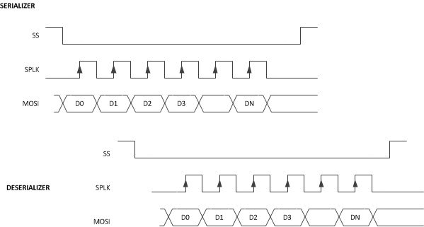
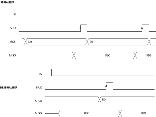
In Forward Channel SPI operation, the SPI master located at the Serializer generates the SPI Clock (SPLK), Master Out / Slave In data (MOSI), and active low Slave Select (SS). The Serializer oversamples the SPI signals directly using the video pixel clock. The three sampled values for SPLK, MOSI, and SS are each sent on data bits in the forward channel frame. At the Deserializer, the SPI signals are regenerated using the pixel clock. To preserve setup and hold time, the Deserializer will hold MOSI data while the SPLK signal is high. In addition, it delays SPLK by one pixel clock relative to the MOSI data, increasing setup by one pixel clock.
 Figure 11. Forward Channel SPI Write
  Figure 12. Forward Channel SPI Read