JAJSI09I September 2009 – October 2019 DS90UR905Q-Q1 , DS90UR906Q-Q1
PRODUCTION DATA.
- 1 特長
- 2 アプリケーション
- 3 概要
- 4 改訂履歴
- 5 概要(続き)
- 6 Pin Configuration and Functions
-
7 Specifications
- 7.1 Absolute Maximum Ratings
- 7.2 ESD Ratings
- 7.3 Recommended Operating Conditions
- 7.4 Thermal Information
- 7.5 Serializer DC Electrical Characteristics
- 7.6 Deserializer DC Electrical Characteristics
- 7.7 DC and AC Serial Control Bus Characteristics
- 7.8 Timing Requirements for DC and AC Serial Control Bus
- 7.9 Timing Requirements for Serializer PCLK
- 7.10 Timing Requirements for Serial Control Bus
- 7.11 Switching Characteristics: Serializer
- 7.12 Switching Characteristics: Deserializer
- 7.13 Typical Characteristics
-
8 Detailed Description
- 8.1 Overview
- 8.2 Functional Block Diagrams
- 8.3
Feature Description
- 8.3.1 Data Transfer
- 8.3.2 Video Control Signal Filter — Serializer and Deserializer
- 8.3.3 Serializer Functional Description
- 8.3.4
Deserializer Functional Description
- 8.3.4.1 Signal Quality Enhancers
- 8.3.4.2 EMI Reduction Features
- 8.3.4.3 Power-Saving Features
- 8.3.4.4 Deserializer CLOCK-DATA RECOVERY STATUS FLAG (LOCK) and OUTPUT STATE SELECT (OSS_SEL)
- 8.3.4.5 Deserializer Oscillator Output (Optional)
- 8.3.4.6 Deserializer OP_LOW (Optional)
- 8.3.4.7 Deserializer Pixel Clock Edge Select (RFB)
- 8.3.4.8 Deserializer Control Signal Filter (Optional)
- 8.3.4.9 Deserializer Low Frequency Optimization (LF_Mode)
- 8.3.4.10 Deserializer Map Select
- 8.3.4.11 Deserializer Strap Input Pins
- 8.3.4.12 Optional Serial Bus Control
- 8.3.4.13 Optional BIST Mode
- 8.3.5 Built-In Self Test (BIST)
- 8.3.6 Optional Serial Bus Control
- 8.4 Device Functional Modes
- 8.5 Register Maps
- 9 Application and Implementation
- 10Power Supply Recommendations
- 11Layout
- 12デバイスおよびドキュメントのサポート
- 13メカニカル、パッケージ、および注文情報
パッケージ・オプション
メカニカル・データ(パッケージ|ピン)
- RHS|48
サーマルパッド・メカニカル・データ
- RHS|48
発注情報
9.2.1 DS90UR905Q-Q1 Typical Connection
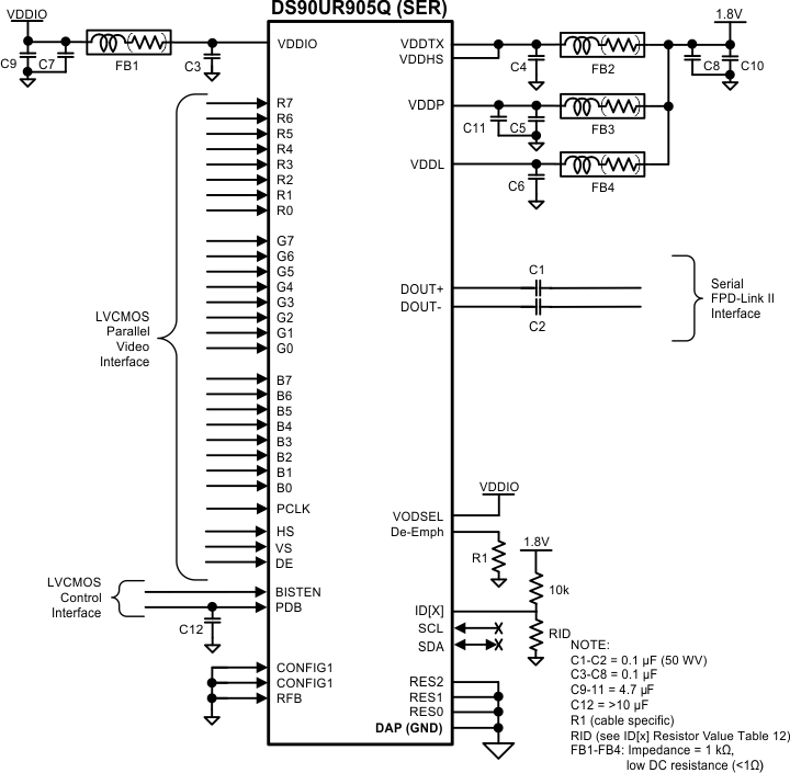
Figure 38 shows a typical application of the DS90UR905Q-Q1 serializer in Pin control mode for a 65 MHz 24-bit Color Display Application. The LVDS outputs require 100-nF AC-coupling capacitors to the line. The line driver includes internal termination. Bypass capacitors are placed near the power supply pins. At a minimum, four 0.1 µF capacitors and a 4.7-µF capacitor should be used for local device bypassing. System GPO (General-Purpose Output) signals control the PDB and BISTEN pins. In this application the RFB pin is tied Low to latch data on the falling edge of the PCLK. The application assumes the companion deserializer (DS90UR906Q-Q1) therefore the configuration pins are also both tied Low. In this example the cable is long, therefore the VODSEL pin is tied High and a De-Emphasis value is selected by the resistor R1. The interface to the host is with 1.8-V LVCMOS levels, thus the VDDIO pin is connected also to the 1.8-V rail. The Optional Serial Bus Control is not used in this example, thus the SCL, SDA and ID[x] pins are left open. A delay cap is placed on the PDB signal to delay the enabling of the device until power is stable.
