JAJSI09I September 2009 – October 2019 DS90UR905Q-Q1 , DS90UR906Q-Q1
PRODUCTION DATA.
- 1 特長
- 2 アプリケーション
- 3 概要
- 4 改訂履歴
- 5 概要(続き)
- 6 Pin Configuration and Functions
-
7 Specifications
- 7.1 Absolute Maximum Ratings
- 7.2 ESD Ratings
- 7.3 Recommended Operating Conditions
- 7.4 Thermal Information
- 7.5 Serializer DC Electrical Characteristics
- 7.6 Deserializer DC Electrical Characteristics
- 7.7 DC and AC Serial Control Bus Characteristics
- 7.8 Timing Requirements for DC and AC Serial Control Bus
- 7.9 Timing Requirements for Serializer PCLK
- 7.10 Timing Requirements for Serial Control Bus
- 7.11 Switching Characteristics: Serializer
- 7.12 Switching Characteristics: Deserializer
- 7.13 Typical Characteristics
-
8 Detailed Description
- 8.1 Overview
- 8.2 Functional Block Diagrams
- 8.3
Feature Description
- 8.3.1 Data Transfer
- 8.3.2 Video Control Signal Filter — Serializer and Deserializer
- 8.3.3 Serializer Functional Description
- 8.3.4
Deserializer Functional Description
- 8.3.4.1 Signal Quality Enhancers
- 8.3.4.2 EMI Reduction Features
- 8.3.4.3 Power-Saving Features
- 8.3.4.4 Deserializer CLOCK-DATA RECOVERY STATUS FLAG (LOCK) and OUTPUT STATE SELECT (OSS_SEL)
- 8.3.4.5 Deserializer Oscillator Output (Optional)
- 8.3.4.6 Deserializer OP_LOW (Optional)
- 8.3.4.7 Deserializer Pixel Clock Edge Select (RFB)
- 8.3.4.8 Deserializer Control Signal Filter (Optional)
- 8.3.4.9 Deserializer Low Frequency Optimization (LF_Mode)
- 8.3.4.10 Deserializer Map Select
- 8.3.4.11 Deserializer Strap Input Pins
- 8.3.4.12 Optional Serial Bus Control
- 8.3.4.13 Optional BIST Mode
- 8.3.5 Built-In Self Test (BIST)
- 8.3.6 Optional Serial Bus Control
- 8.4 Device Functional Modes
- 8.5 Register Maps
- 9 Application and Implementation
- 10Power Supply Recommendations
- 11Layout
- 12デバイスおよびドキュメントのサポート
- 13メカニカル、パッケージ、および注文情報
7.12 Switching Characteristics: Deserializer
over recommended operating supply and temperature ranges unless otherwise specified.| PARAMETERS | TEST CONDITIONS | PIN / FREQ | MIN | TYP | MAX | UNIT | |
|---|---|---|---|---|---|---|---|
| tRCP | PCLK output period | tRCP = tTCP | PCLK | 15.38 | T | 200 | ns |
| tRDC | PCLK output duty cycle | SSCG=OFF, 5–65 MHz | PCLK | 43% | 50% | 57% | |
| SSCG=ON, 5–20 MHz | 35% | 59% | 65% | ||||
| SSCG=ON, 20–65 MHz | 40% | 53% | 60% | ||||
| tCLH | LVCMOS
Low-to-high transition time, Figure 10 |
VDDIO = 1.8 V, CL = 4 pF | PCLK/RGB[7:0], HS, VS, DE | 2.1 | ns | ||
| VDDIO = 3.3 V, CL = 4 pF | 2.0 | ns | |||||
| tCHL | LVCMOS
High-to-low transition time, Figure 10 |
VDDIO = 1.8 V
CL = 4 pF, OS_PCLK/DATA = L |
PCLK/RGB[7:0], HS, VS, DE | 1.6 | ns | ||
| VDDIO = 3.3 V
CL = 4 pF, OS_PCLK/DATA = H |
1.5 | ns | |||||
| tROS | Data valid before PCLK – set-up time Figure 14 | VDDIO = 1.71 to 1.89 V or 3.0 to 3.6 V
CL = 4pF (lumped load) |
RGB[7:0], HS, VS, DE | 0.27 | 0.45 | T | |
| tROH | Data valid after PCLK – hold time Figure 14 | VDDIO = 1.71 to 1.89 V or 3.0 to 3.6 V
CL = 4pF (lumped load) |
RGB[7:0], HS, VS, DE | 0.4 | 0.55 | T | |
| tDDLT(2) | Deserializer lock time,
Figure 13 |
SSC[3:0] = 0000 (OFF)(1) | PCLK = 5 MHz | 3 | ms | ||
| SSC[3:0] = 0000 (OFF)(1) | PCLK = 65 MHz | 4 | ms | ||||
| SSC[3:0] = ON(1) | PCLK = 5 MHz | 30 | ms | ||||
| SSC[3:0] = ON(1) | PCLK = 65 MHz | 6 | ms | ||||
| tDD | Deserializer delay – latency, Figure 11 | SSC[3:0] = 0000 (OFF)(1) | 139 × T | 140 × T | ns | ||
| tDPJ | Deserializer period jitter | SSC[3:0] = OFF(3)(5)(6) | PCLK = 5 MHz | 975 | 1700 | ps | |
| PCLK = 10 MHz | 500 | 1000 | ps | ||||
| PCLK = 65 MHz | 550 | 1250 | ps | ||||
| tDCCJ | Deserializer cycle-to-cycle jitter | SSC[3:0] = OFF(3)(4)(6) | PCLK = 5 MHz | 675 | 1150 | ps | |
| PCLK = 10 MHz | 375 | 900 | ps | ||||
| PCLK = 65 MHz | 500 | 1150 | ps | ||||
| tIJT | Deserializer input jitter tolerance, Figure 16 | EQ = OFF,
SSCG = OFF, PCLK = 65 MHz |
for jitter freq < 2 MHz | 0.9 | UI | ||
| for jitter freq > 6 MHz | 0.5 | UI | |||||
| BIST Mode | |||||||
| tPASS | BIST PASS valid time,
BISTEN = 1, Figure 17 |
1 | 10 | µs | |||
| SSCG Mode | |||||||
| fDEV | Spread spectrum clocking deviation frequency | Under typical conditions | PCLK = 5 to 65 MHz,
SSC[3:0] = ON |
±0.5% | ±2% | ||
| fMOD | Spread spectrum clocking modulation frequency | Under typical conditions | PCLK = 5 to 65 MHz,
SSC[3:0] = ON |
8 | 100 | kHz | |
(1) tPLD is the time required by the serializer to obtain lock when exiting power-down state with an active PCLK.
(2) tDDLT is the time required by the deserializer to obtain lock when exiting power-down state with an active PCLK.
(3) tDPJ is the maximum amount the period is allowed to deviate over many samples.
(4) tDCCJ is the maximum amount of jitter between adjacent clock cycles.
(5) Specification is ensured by characterization and is not tested in production.
(6) Specification is ensured by design and is not tested in production.
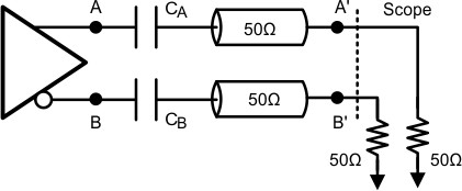 Figure 1. Serializer Test Circuit
 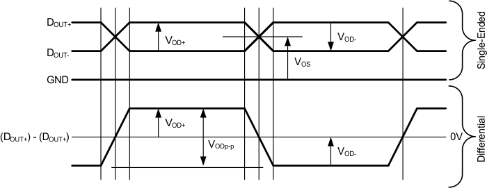 Figure 2. Serializer Output Waveforms
  Figure 3. Serializer Output Transition Times
  Figure 4. Serializer Input PCLK Waveform and Set and Hold Times
 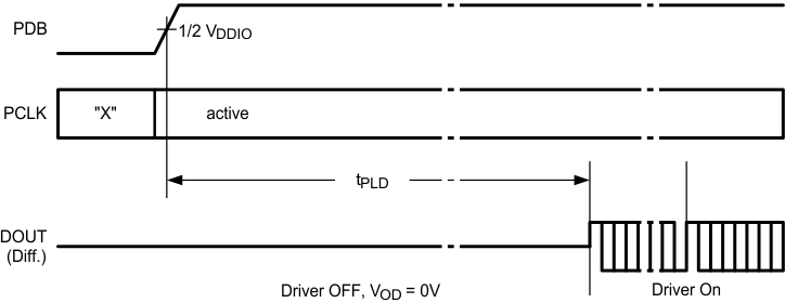 Figure 5. Serializer Lock Time
 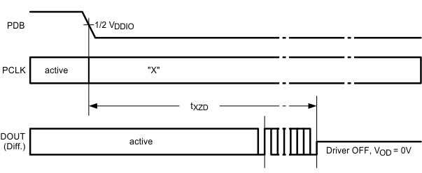 Figure 6. Serializer Disable Time
  Figure 7. Serializer Latency Delay
 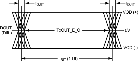 Figure 8. Serializer Output Jitter
 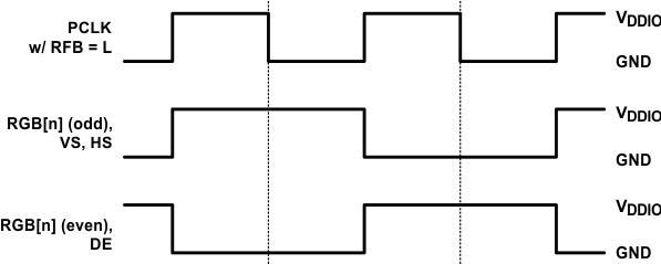 Figure 9. Checkerboard Data Pattern
  Figure 10. Deserializer LVCMOS Transition Times
  Figure 11. Deserializer Delay – Latency
 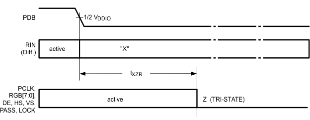 Figure 12. Deserializer Disable Time (OSS_SEL = 0)
 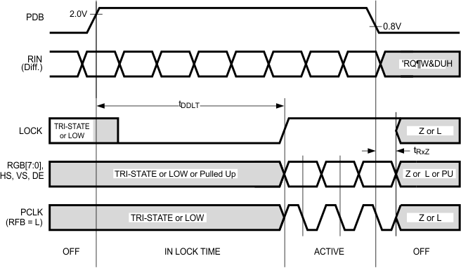 Figure 13. Deserializer PLL Lock Times and PDB TRI-STATE Delay
  Figure 15. Deserializer Output Data Valid (Set-up and Hold) Times With SSCG = On
 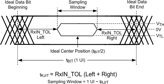 Figure 16. Receiver Input Jitter Tolerance
  Figure 17. BIST PASS Waveform
  Figure 18. Serial Control Bus Timing Diagram