JAJSI09I September 2009 – October 2019 DS90UR905Q-Q1 , DS90UR906Q-Q1
PRODUCTION DATA.
- 1 特長
- 2 アプリケーション
- 3 概要
- 4 改訂履歴
- 5 概要(続き)
- 6 Pin Configuration and Functions
-
7 Specifications
- 7.1 Absolute Maximum Ratings
- 7.2 ESD Ratings
- 7.3 Recommended Operating Conditions
- 7.4 Thermal Information
- 7.5 Serializer DC Electrical Characteristics
- 7.6 Deserializer DC Electrical Characteristics
- 7.7 DC and AC Serial Control Bus Characteristics
- 7.8 Timing Requirements for DC and AC Serial Control Bus
- 7.9 Timing Requirements for Serializer PCLK
- 7.10 Timing Requirements for Serial Control Bus
- 7.11 Switching Characteristics: Serializer
- 7.12 Switching Characteristics: Deserializer
- 7.13 Typical Characteristics
-
8 Detailed Description
- 8.1 Overview
- 8.2 Functional Block Diagrams
- 8.3
Feature Description
- 8.3.1 Data Transfer
- 8.3.2 Video Control Signal Filter — Serializer and Deserializer
- 8.3.3 Serializer Functional Description
- 8.3.4
Deserializer Functional Description
- 8.3.4.1 Signal Quality Enhancers
- 8.3.4.2 EMI Reduction Features
- 8.3.4.3 Power-Saving Features
- 8.3.4.4 Deserializer CLOCK-DATA RECOVERY STATUS FLAG (LOCK) and OUTPUT STATE SELECT (OSS_SEL)
- 8.3.4.5 Deserializer Oscillator Output (Optional)
- 8.3.4.6 Deserializer OP_LOW (Optional)
- 8.3.4.7 Deserializer Pixel Clock Edge Select (RFB)
- 8.3.4.8 Deserializer Control Signal Filter (Optional)
- 8.3.4.9 Deserializer Low Frequency Optimization (LF_Mode)
- 8.3.4.10 Deserializer Map Select
- 8.3.4.11 Deserializer Strap Input Pins
- 8.3.4.12 Optional Serial Bus Control
- 8.3.4.13 Optional BIST Mode
- 8.3.5 Built-In Self Test (BIST)
- 8.3.6 Optional Serial Bus Control
- 8.4 Device Functional Modes
- 8.5 Register Maps
- 9 Application and Implementation
- 10Power Supply Recommendations
- 11Layout
- 12デバイスおよびドキュメントのサポート
- 13メカニカル、パッケージ、および注文情報
8.3.5.1 Sample BIST Sequence
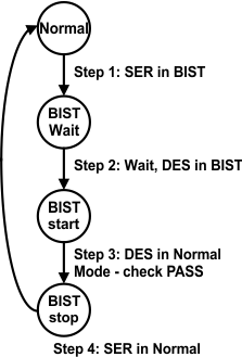
See Figure 32 for the BIST mode flow diagram.
Step 1: Place the DS90UR905Q-Q1 serializer in BIST Mode by setting serializer BISTEN = H. For the DS90UR905Q-Q1 serializer or DS99R421 FPD-Link II serializer BIST Mode is enabled through the BISTEN pin. For the DS90C241 serializer or DS90UR241 serializer, BIST mode is enetered by setting all the input data of the device to LOW state. A PCLK is required for all the serializer options. When the deserializer detects the BIST mode pattern and command (DCA and DCB code) the RGB and control signal outputs are shut off.
Step 2: Place the DS90UR906Q-Q1 deserializer in BIST mode by setting the BISTEN = H. The deserializer is now in the BIST mode and checks the incoming serial payloads for errors. If an error in the payload (1 to 24) is detected, the PASS pin will switch low for one half of the clock period. During the BIST test, the PASS output can be monitored and counted to determine the payload error rate.
Step 3: To Stop the BIST mode, the deserializer BISTEN pin is set Low. The deserializer stops checking the data and the final test result is held on the PASS pin. If the test ran error free, the PASS output will be High. If there was one or more errors detected, the PASS output will be Low. The PASS output state is held until a new BIST is run, the device is RESET, or Powered Down. The BIST duration is user controlled by the duration of the BISTEN signal.
Step 4: To return the link to normal operation, the serializer BISTEN input is set Low. The Link returns to normal operation.
Figure 33 shows the waveform diagram of a typical BIST test for two cases. Case 1 is error free, and Case 2 shows one with multiple errors. In most cases it is difficult to generate errors due to the robustness of the link (differential data transmission etc.), thus they may be introduced by greatly extending the cable length, faulting the interconnect, reducing signal condition enhancements (De-Emphasis, VODSEL, or Rx Equalization).
 Figure 32. BIST Mode Flow Diagram