SNLS414E June 2012 – October 2016 DS90UR910-Q1
PRODUCTION DATA.
- 1 Features
- 2 Applications
- 3 Description
- 4 Revision History
- 5 Pin Configuration and Functions
-
6 Specifications
- 6.1 Absolute Maximum Ratings
- 6.2 ESD Ratings
- 6.3 Recommended Operating Conditions
- 6.4 Thermal Information
- 6.5 Electrical Characteristics: DC
- 6.6 Switching Characteristics: AC
- 6.7 Timing Requirements: Serial Control Bus (CCI and I2C)
- 6.8 Timing Requirements: DC and AC Serial Control Bus (CCI and I2C)
- 6.9 Typical Characteristics
- 7 Detailed Description
- 8 Application and Implementation
- 9 Power Supply Recommendations
- 10Layout
- 11Device and Documentation Support
- 12Mechanical, Packaging, and Orderable Information
パッケージ・オプション
メカニカル・データ(パッケージ|ピン)
- RTA|40
サーマルパッド・メカニカル・データ
- RTA|40
発注情報
8 Application and Implementation
NOTE
Information in the following applications sections is not part of the TI component specification, and TI does not warrant its accuracy or completeness. TI’s customers are responsible for determining suitability of components for their purposes. Customers should validate and test their design implementation to confirm system functionality.
8.1 Application Information
The DS90UR910-Q1 device recovers data from the FPD-Link II serial bit stream and converts into CSI-2. The recovered data is packetized and serialized over two data lanes strobed by a half-rate serial clock compliant with the MIPI DPHY and CSI-2 specifications, each running up to 900 Mbps. The FPD-Link II receiver supports pixel clocks of up to 75 MHz. The CSI-2 output serial bus greatly reduces the interconnect and signal count to a graphic processing unit (GPU) and eases system designs for video streams from multiple automotive driver assist cameras.
8.2 Typical Application
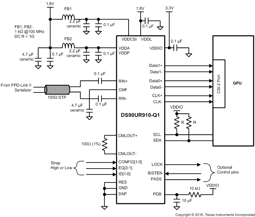
 Figure 16. DS90UR910-Q1 Typical Connection Diagram — Pin Control
8.2.1 Design Requirements
For this typical design application, Table 8 lists the input parameters.
Table 8. Design Parameters
| PARAMETER | VALUE |
|---|---|
| VDDIO | 1.8 V or 3.3 V |
| VDDL, VDDA, VDDP, VDDCSI | 1.8 V |
| AC-coupling capacitor for RIN0± and RIN1± | 100 nF |
8.2.2 Detailed Design Procedure
Figure 16 shows a typical application of the DS90UR910-Q1 in Pin control mode for a 24-bit Color Display Application. The LVDS signals require 100-nF AC-coupling capacitors to the line. The line driver includes internal termination. Bypass capacitors are placed near the power supply pins. At a minimum, four 0.1-µF capacitors and a 4.7-µF capacitor must be used for local device bypassing. System GPO (General Purpose Output) signals control the PDB and BISTEN pins. The interface to the host is with 1.8-V LVCMOS levels, thus the VDDIO pin is connected also to the 1.8-V rail. The optional I2C or CCI is connected to the Host bus in this example, thus the SCL and SDA pins are using pullup resistors R to VDDIO. A delay cap is placed on the PDB signal to delay the enabling of the device until power is stable.
The SER/DES supports only AC-coupled interconnects through an integrated DC-balanced decoding scheme. External AC-coupling capacitors must be placed in series in the FPD-Link II signal path as illustrated in Figure 17.
 Figure 17. AC-Coupled Connection
For high-speed FPD-Link II transmissions, the smallest available package must be used for the AC coupling capacitor. This helps minimize degradation of signal quality due to package parasitics. The inputs and outputs require 100-nF AC-coupling capacitors to the line.
8.2.3 Application Curves
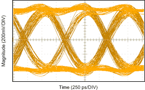
Figure 18 corresponds to 49-MHz PCLK UNH pattern.
 Figure 18. Loop-Through CML Output at 1.372-Gbps Serial Line Rate