JAJSFV0 July 2018 ESD351
PRODUCTION DATA.
6.7 Typical Characteristics
 Figure 1. TLP I-V Curve, I/O Pin to GND (tp = 100 ns)
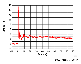
  Figure 3. 8-kV IEC 61000-4-2 Clamping Voltage, I/O pin to GND
  Figure 5. Surge Curve (IEC 61000-4-5, tp = 8/20 µs), I/O Pin to GND
  Figure 7. Leakage Current at 3.6 V Bias Voltage Across Temperature, I/O Pin to GND
  Figure 9. Insertion Loss Vs. Frequency
  Figure 2. TLP I/V Curve, GND to I/O Pin (tp = 100 ns)
  Figure 4. 8-kV IEC 61000-4-2 Clamping Voltage, GND to I/O Pin
  Figure 6. DC IV-Curve, I/O Pin to GND
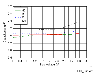
  Figure 8. Capacitance Vs. Bias Voltage at Different Temperatures (°C)