JAJSDM6A July   2017  – July 2017 ESD401

PRODUCTION DATA.  

  1. 特長
  2. アプリケーション
  3. 概要
  4. 改訂履歴
  5. Pin Configuration and Functions
  6. Specifications
    1. 6.1 Absolute Maximum Ratings
    2. 6.2 ESD Ratings — JEDEC Specification 
    3. 6.3 ESD Ratings—IEC Specification
    4. 6.4 Recommended Operating Conditions
    5. 6.5 Thermal Information
    6. 6.6 Electrical Characteristics
    7. 6.7 Typical Characteristics
  7. Detailed Description
    1. 7.1 Overview
    2. 7.2 Functional Block Diagram
    3. 7.3 Feature Description
      1. 7.3.1 IEC 61000-4-2 ESD Protection
      2. 7.3.2 IEC 61000-4-4 EFT Protection
      3. 7.3.3 IEC 61000-4-5 Surge Protection
      4. 7.3.4 IO Capacitance
      5. 7.3.5 DC Breakdown Voltage
      6. 7.3.6 Low Leakage Current
      7. 7.3.7 Low ESD Clamping Voltage
      8. 7.3.8 Industrial Temperature Range
      9. 7.3.9 Industry Standard Footprint
    4. 7.4 Device Functional Modes
  8. Application and Implementation
    1. 8.1 Application Information
    2. 8.2 Typical Application
      1. 8.2.1 Design Requirements
      2. 8.2.2 Detailed Design Procedure
        1. 8.2.2.1 Signal Range
        2. 8.2.2.2 Operating Frequency
      3. 8.2.3 Application Curves
  9. Power Supply Recommendations
  10. 10Layout
    1. 10.1 Layout Guidelines
    2. 10.2 Layout Example
  11. 11デバイスおよびドキュメントのサポート
    1. 11.1 ドキュメントのサポート
    2. 11.2 ドキュメントの更新通知を受け取る方法
    3. 11.3 コミュニティ・リソース
    4. 11.4 商標
    5. 11.5 静電気放電に関する注意事項
    6. 11.6 Glossary
  12. 12メカニカル、パッケージ、および注文情報

パッケージ・オプション

メカニカル・データ(パッケージ|ピン)
サーマルパッド・メカニカル・データ
発注情報

Layout

Layout Guidelines

  • The optimum placement is as close to the connector as possible.
    • EMI during an ESD event can couple from the trace being struck to other nearby unprotected traces, resulting in early system failures.
    • The PCB designer must minimize the possibility of EMI coupling by keeping any unprotected traces away from the protected traces which are between the TVS and the connector.
  • Route the protected traces as straight as possible.
  • Eliminate any sharp corners on the protected traces between the TVS and the connector by using rounded corners with the largest radii possible.
    • Electric fields tend to build up on corners, increasing EMI coupling.

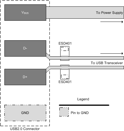
Layout Example

ESD401 Layout_ESD401.gif Figure 16. USB 2.0 ESD Layout