JAJSDM6B July 2017 – August 2024 ESD401
PRODUCTION DATA
- 1
- 1 特長
- 2 アプリケーション
- 3 概要
- 4 Pin Configuration and Functions
- 5 Specifications
- 6 Detailed Description
- 7 Application and Implementation
- 8 Device and Documentation Support
- 9 Revision History
- 10Mechanical, Packaging, and Orderable Information
- 11Mechanical Data
5.7 Typical Characteristics
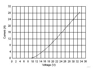 Figure 5-1 Positive TLP Curve, Pin 1 to Pin 2
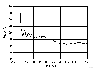 Figure 5-3 8-kV IEC 61000-4-2 Waveform, Pin1 to Pin 2
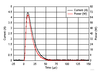 Figure 5-5 Surge (IEC 61000-4-5) Curve (tp = 8/20 µs), Pin 1 to Pin 2
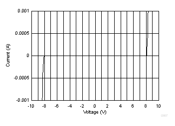 Figure 5-7 DC Voltage Sweep I-V Curve, Pin 1 to Pin 2
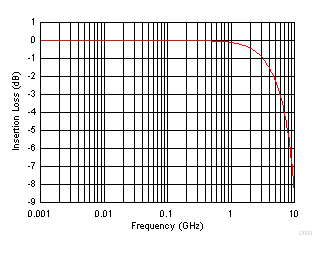 Figure 5-9 Insertion Loss
 Figure 5-2 Negative TLP Curve, Pin 1 to Pin 2 (Plotted as Positive TLP Curve Pin 2 to Pin 1
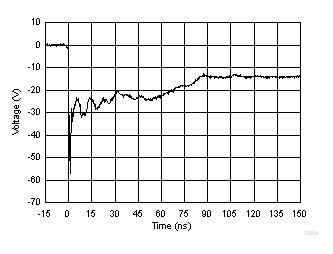 Figure 5-4 –8-kV IEC 61000-4-2 Waveform, Pin 1 to Pin 2
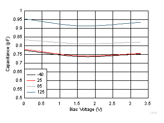 Figure 5-6 Capacitance vs Bias Voltage, Pin 1 to Pin 2
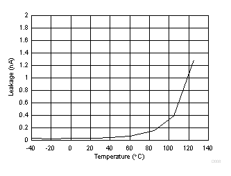 Figure 5-8 Leakage Current vs. Temperature, Pin 1 to Pin 2
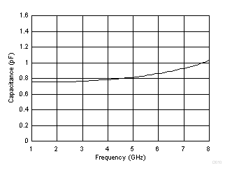 Figure 5-10 Capacitance vs. Frequency, Pin 1 to Pin 2