SPRS825F October   2012  – June 2020 F28M36H33B2 , F28M36H53B2 , F28M36P53C2 , F28M36P63C2

PRODUCTION DATA.  

  1. 1Device Overview
    1. 1.1 Features
    2. 1.2 Applications
    3. 1.3 Description
    4. 1.4 Functional Block Diagram
  2. 2Revision History
  3. 3Device Comparison
    1. 3.1 Related Products
  4. 4Terminal Configuration and Functions
    1. 4.1 Pin Diagrams
    2. 4.2 Signal Descriptions
      1. Table 4-1 Signal Descriptions
  5. 5Specifications
    1. 5.1  Absolute Maximum Ratings
    2. 5.2  ESD Ratings – Commercial
    3. 5.3  Recommended Operating Conditions
    4. 5.4  Power Consumption Summary
      1. Table 5-1 Current Consumption at 150-MHz C28x SYSCLKOUT and 75-MHz M3SSCLK
      2. Table 5-2 Current Consumption at 125-MHz C28x SYSCLKOUT and 125-MHz M3SSCLK
    5. 5.5  Electrical Characteristics
    6. 5.6  Thermal Resistance Characteristics for ZWT Package (Revision 0 Silicon)
    7. 5.7  Thermal Resistance Characteristics for ZWT Package (Revision A Silicon)
    8. 5.8  Thermal Design Considerations
    9. 5.9  Timing and Switching Characteristics
      1. 5.9.1 Power Sequencing
        1. Table 5-3 Reset (XRS) Timing Requirements
        2. Table 5-4 Reset (XRS) Switching Characteristics
        3. 5.9.1.1   Power Management and Supervisory Circuit Solutions
      2. 5.9.2 Clock Specifications
        1. 5.9.2.1 Changing the Frequency of the Main PLL
        2. 5.9.2.2 Input Clock Frequency and Timing Requirements, PLL Lock Times
          1. Table 5-5  Input Clock Frequency
          2. Table 5-7  Crystal Oscillator Electrical Characteristics
          3. Table 5-8  X1 Timing Requirements - PLL Enabled
          4. Table 5-9  X1 Timing Requirements - PLL Disabled
          5. Table 5-10 XCLKIN Timing Requirements - PLL Enabled
          6. Table 5-11 XCLKIN Timing Requirements - PLL Disabled
          7. Table 5-12 PLL Lock Times
        3. 5.9.2.3 Output Clock Frequency and Switching Characteristics
          1. Table 5-13 Output Clock Frequency
          2. Table 5-14 XCLKOUT Switching Characteristics (PLL Bypassed or Enabled)
        4. 5.9.2.4 Internal Clock Frequencies
          1. Table 5-15 Internal Clock Frequencies (150-MHz Devices)
      3. 5.9.3 Timing Parameter Symbology
        1. 5.9.3.1 General Notes on Timing Parameters
        2. 5.9.3.2 Test Load Circuit
      4. 5.9.4 Flash Timing – Master Subsystem
        1. Table 5-16 Master Subsystem – Flash/OTP Endurance
        2. Table 5-17 Master Subsystem – Flash Parameters
        3. Table 5-18 Master Subsystem – Flash/OTP Access Timing
        4. Table 5-19 Master Subsystem – Flash Data Retention Duration
      5. 5.9.5 Flash Timing – Control Subsystem
        1. Table 5-21 Control Subsystem – Flash/OTP Endurance
        2. Table 5-22 Control Subsystem – Flash Parameters
        3. Table 5-23 Control Subsystem – Flash/OTP Access Timing
        4. Table 5-24 Control Subsystem – Flash Data Retention Duration
      6. 5.9.6 GPIO Electrical Data and Timing
        1. 5.9.6.1 GPIO - Output Timing
          1. Table 5-26 General-Purpose Output Switching Characteristics
        2. 5.9.6.2 GPIO - Input Timing
          1. Table 5-27 General-Purpose Input Timing Requirements
        3. 5.9.6.3 Sampling Window Width for Input Signals
        4. 5.9.6.4 Low-Power Mode Wakeup Timing
          1. Table 5-28 IDLE Mode Timing Requirements
          2. Table 5-29 IDLE Mode Switching Characteristics
          3. Table 5-30 STANDBY Mode Timing Requirements
          4. Table 5-31 STANDBY Mode Switching Characteristics
          5. Table 5-32 HALT Mode Timing Requirements
          6. Table 5-33 HALT Mode Switching Characteristics
      7. 5.9.7 External Interrupt Electrical Data and Timing
        1. Table 5-34 External Interrupt Timing Requirements
        2. Table 5-35 External Interrupt Switching Characteristics
    10. 5.10 Analog and Shared Peripherals
      1. 5.10.1 Analog-to-Digital Converter
        1. 5.10.1.1 Sample Mode
        2. 5.10.1.2 Start-of-Conversion Triggers
        3. 5.10.1.3 Analog Inputs
        4. 5.10.1.4 ADC Result Registers and EOC Interrupts
        5. 5.10.1.5 ADC Electrical Data and Timing
          1. Table 5-36 ADC Electrical Characteristics
          2. Table 5-37 External ADC Start-of-Conversion Switching Characteristics
      2. 5.10.2 Comparator + DAC Units
        1. 5.10.2.1 On-Chip Comparator and DAC Electrical Data and Timing
          1. Table 5-38 Electrical Characteristics of the Comparator/DAC
      3. 5.10.3 Interprocessor Communications
      4. 5.10.4 External Peripheral Interface
        1. 5.10.4.1 EPI General-Purpose Mode
        2. 5.10.4.2 EPI SDRAM Mode
        3. 5.10.4.3 EPI Host Bus Mode
          1. 5.10.4.3.1 EPI 8-Bit Host Bus (HB-8) Mode
            1. 5.10.4.3.1.1 HB-8 Muxed Address/Data Mode
            2. 5.10.4.3.1.2 HB-8 Non-Muxed Address/Data Mode
            3. 5.10.4.3.1.3 HB-8 FIFO Mode
          2. 5.10.4.3.2 EPI 16-Bit Host Bus (HB-16) Mode
            1. 5.10.4.3.2.1 HB-16 Muxed Address/Data Mode
            2. 5.10.4.3.2.2 HB-16 Non-Muxed Address/Data Mode
            3. 5.10.4.3.2.3 HB-16 FIFO Mode
        4. 5.10.4.4 EPI Electrical Data and Timing
          1. Table 5-52 EPI SDRAM Interface Switching Characteristics (see , , and )
          2. Table 5-53 EPI Host-Bus 8 and Host-Bus 16 Interface Switching Characteristics (see , , , and )
          3. Table 5-54 EPI Host-Bus 8 and Host-Bus 16 Interface Timing Requirements (see and )
          4. Table 5-55 EPI General-Purpose Interface Switching Characteristics (see )
          5. Table 5-56 EPI General-Purpose Interface Timing Requirements (see and )
    11. 5.11 Master Subsystem Peripherals
      1. 5.11.1 Synchronous Serial Interface
        1. 5.11.1.1 Bit Rate Generation
        2. 5.11.1.2 Transmit FIFO
        3. 5.11.1.3 Receive FIFO
        4. 5.11.1.4 Interrupts
        5. 5.11.1.5 Frame Formats
      2. 5.11.2 Universal Asynchronous Receiver/Transmitter
        1. 5.11.2.1 Baud-Rate Generation
        2. 5.11.2.2 Transmit and Receive Logic
        3. 5.11.2.3 Data Transmission and Reception
        4. 5.11.2.4 Interrupts
      3. 5.11.3 Cortex-M3 Inter-Integrated Circuit
        1. 5.11.3.1 Functional Overview
        2. 5.11.3.2 Available Speed Modes
        3. 5.11.3.3 I2C Electrical Data and Timing
          1. Table 5-57 I2C Timing
      4. 5.11.4 Cortex-M3 Controller Area Network
        1. 5.11.4.1 Functional Overview
      5. 5.11.5 Cortex-M3 Universal Serial Bus Controller
        1. 5.11.5.1 Functional Description
      6. 5.11.6 Cortex-M3 Ethernet Media Access Controller
        1. 5.11.6.1 Functional Overview
        2. 5.11.6.2 MII Signals
        3. 5.11.6.3 EMAC Electrical Data and Timing
          1. Table 5-59 Timing Requirements for MIITXCK (see )
          2. Table 5-60 Timing Requirements for MIIRXCK (see )
          3. Table 5-61 Switching Characteristics for EMAC MII Transmit (see )
          4. Table 5-62 Timing Requirements for EMAC MII Receive (see )
        4. 5.11.6.4 MDIO Electrical Data and Timing
          1. Table 5-63 Switching Characteristics for MDIO_CK (see )
          2. Table 5-64 Switching Characteristics for MDIO as Output (see )
          3. Table 5-65 Timing Requirements for MDIO as Input (see )
    12. 5.12 Control Subsystem Peripherals
      1. 5.12.1 High-Resolution PWM and Enhanced PWM Modules
        1. 5.12.1.1 HRPWM Electrical Data and Timing
          1. Table 5-66 High-Resolution PWM Characteristics at SYSCLKOUT = (60–150 MHz)
        2. 5.12.1.2 ePWM Electrical Data and Timing
          1. Table 5-67 ePWM Timing Requirements
          2. Table 5-68 ePWM Switching Characteristics
          3. 5.12.1.2.1 Trip-Zone Input Timing
            1. Table 5-69 Trip-Zone Input Timing Requirements
      2. 5.12.2 Enhanced Capture Module
        1. 5.12.2.1 eCAP Electrical Data and Timing
          1. Table 5-70 eCAP Timing Requirement
          2. Table 5-71 eCAP Switching Characteristics
      3. 5.12.3 Enhanced Quadrature Encoder Pulse Module
        1. 5.12.3.1 eQEP Electrical Data and Timing
          1. Table 5-72 eQEP Timing Requirements
          2. Table 5-73 eQEP Switching Characteristics
      4. 5.12.4 C28x Inter-Integrated Circuit Module
        1. 5.12.4.1 Functional Overview
        2. 5.12.4.2 Clock Generation
        3. 5.12.4.3 I2C Electrical Data and Timing
          1. Table 5-74 I2C Timing
      5. 5.12.5 C28x Serial Communications Interface
        1. 5.12.5.1 Architecture
        2. 5.12.5.2 Multiprocessor and Asynchronous Communication Modes
      6. 5.12.6 C28x Serial Peripheral Interface
        1. 5.12.6.1 Functional Overview
        2. 5.12.6.2 SPI Electrical Data and Timing
          1. 5.12.6.2.1 Master Mode Timing
            1. Table 5-75 SPI Master Mode External Timing (Clock Phase = 0)
            2. Table 5-76 SPI Master Mode External Timing (Clock Phase = 1)
          2. 5.12.6.2.2 Slave Mode Timing
            1. Table 5-77 SPI Slave Mode External Timing (Clock Phase = 0)
            2. Table 5-78 SPI Slave Mode External Timing (Clock Phase = 1)
      7. 5.12.7 C28x Multichannel Buffered Serial Port
        1. 5.12.7.1 McBSP Electrical Data and Timing
          1. 5.12.7.1.1 McBSP Transmit and Receive Timing
            1. Table 5-79 McBSP Timing Requirements
            2. Table 5-80 McBSP Switching Characteristics
          2. 5.12.7.1.2 McBSP as SPI Master or Slave Timing
            1. Table 5-81 McBSP as SPI Master or Slave Timing Requirements (CLKSTP = 10b, CLKXP = 0)
            2. Table 5-82 McBSP as SPI Master or Slave Switching Characteristics (CLKSTP = 10b, CLKXP = 0)
            3. Table 5-83 McBSP as SPI Master or Slave Timing Requirements (CLKSTP = 11b, CLKXP = 0)
            4. Table 5-84 McBSP as SPI Master or Slave Switching Characteristics (CLKSTP = 11b, CLKXP = 0)
            5. Table 5-85 McBSP as SPI Master or Slave Timing Requirements (CLKSTP = 10b, CLKXP = 1)
            6. Table 5-86 McBSP as SPI Master or Slave Switching Characteristics (CLKSTP = 10b, CLKXP = 1)
            7. Table 5-87 McBSP as SPI Master or Slave Timing Requirements (CLKSTP = 11b, CLKXP = 1)
            8. Table 5-88 McBSP as SPI Master or Slave Switching Characteristics (CLKSTP = 11b, CLKXP = 1)
  6. 6Detailed Description
    1. 6.1  Memory Maps
      1. 6.1.1 Control Subsystem Memory Map
      2. 6.1.2 Master Subsystem Memory Map
    2. 6.2  Identification
    3. 6.3  Master Subsystem
      1. 6.3.1 Cortex-M3 CPU
      2. 6.3.2 Cortex-M3 DMA and NVIC
      3. 6.3.3 Cortex-M3 Interrupts
      4. 6.3.4 Cortex-M3 Vector Table
      5. 6.3.5 Cortex-M3 Local Peripherals
      6. 6.3.6 Cortex-M3 Local Memory
      7. 6.3.7 Cortex-M3 Accessing Shared Resources and Analog Peripherals
    4. 6.4  Control Subsystem
      1. 6.4.1 C28x CPU/FPU/VCU
      2. 6.4.2 C28x Core Hardware Built-In Self-Test
      3. 6.4.3 C28x Peripheral Interrupt Expansion
      4. 6.4.4 C28x Direct Memory Access
      5. 6.4.5 C28x Local Peripherals
      6. 6.4.6 C28x Local Memory
      7. 6.4.7 C28x Accessing Shared Resources and Analog Peripherals
    5. 6.5  Analog Subsystem
      1. 6.5.1 ADC1
      2. 6.5.2 ADC2
      3. 6.5.3 Analog Comparator + DAC
      4. 6.5.4 Analog Common Interface Bus
    6. 6.6  Master Subsystem NMIs
    7. 6.7  Control Subsystem NMIs
    8. 6.8  Resets
      1. 6.8.1 Cortex-M3 Resets
      2. 6.8.2 C28x Resets
      3. 6.8.3 Analog Subsystem and Shared Resources Resets
      4. 6.8.4 Device Boot Sequence
    9. 6.9  Internal Voltage Regulation and Power-On-Reset Functionality
      1. 6.9.1 Analog Subsystem: Internal 1.8-V VREG
      2. 6.9.2 Digital Subsystem: Internal 1.2-V VREG
      3. 6.9.3 Analog and Digital Subsystems: Power-On-Reset Functionality
      4. 6.9.4 Connecting ARS and XRS Pins
    10. 6.10 Input Clocks and PLLs
      1. 6.10.1 Internal Oscillator (Zero-Pin)
      2. 6.10.2 Crystal Oscillator/Resonator (Pins X1/X2 and VSSOSC)
      3. 6.10.3 External Oscillators (Pins X1, VSSOSC, XCLKIN)
      4. 6.10.4 Main PLL
      5. 6.10.5 USB PLL
    11. 6.11 Master Subsystem Clocking
      1. 6.11.1 Cortex-M3 Run Mode
      2. 6.11.2 Cortex-M3 Sleep Mode
      3. 6.11.3 Cortex-M3 Deep Sleep Mode
    12. 6.12 Control Subsystem Clocking
      1. 6.12.1 C28x Normal Mode
      2. 6.12.2 C28x IDLE Mode
      3. 6.12.3 C28x STANDBY Mode
    13. 6.13 Analog Subsystem Clocking
    14. 6.14 Shared Resources Clocking
    15. 6.15 Loss of Input Clock (NMI Watchdog Function)
    16. 6.16 GPIOs and Other Pins
      1. 6.16.1 GPIO_MUX1
      2. 6.16.2 GPIO_MUX2
      3. 6.16.3 AIO_MUX1
      4. 6.16.4 AIO_MUX2
    17. 6.17 Emulation/JTAG
    18. 6.18 Code Security Module
      1. 6.18.1 Functional Description
    19. 6.19 µCRC Module
      1. 6.19.1 Functional Description
      2. 6.19.2 CRC Polynomials
      3. 6.19.3 CRC Calculation Procedure
      4. 6.19.4 CRC Calculation for Data Stored In Secure Memory
  7. 7Applications, Implementation, and Layout
    1. 7.1 TI Reference Design
  8. 8Device and Documentation Support
    1. 8.1 Device and Development Support Tool Nomenclature
    2. 8.2 Tools and Software
    3. 8.3 Documentation Support
    4. 8.4 Related Links
    5. 8.5 Support Resources
    6. 8.6 Trademarks
    7. 8.7 Electrostatic Discharge Caution
    8. 8.8 Glossary
  9. 9Mechanical, Packaging, and Orderable Information
    1. 9.1 Packaging Information

パッケージ・オプション

メカニカル・データ(パッケージ|ピン)
サーマルパッド・メカニカル・データ
発注情報

Master Subsystem Clocking

The internal PLLSYSCLK clock, normally used as a source for all Master Subsystem clocks, is a divided-down output of the Main PLL or X1 external clock input, as defined by the SPLLCKEN bit of the SYSPLLCTL register.

There is also a second oscillator that internally generates two clocks: 32KHZCLK and 10MHZCLK. The 10MHZCLK is used by the Missing Clock Circuit to detect a possible absence of an external clock source to the Main Oscillator that drives the Main PLL. Detection of a missing clock results in a substitution of the 10MHZCLK for the PLLSYSCLK. The CLKFAIL signal is also sent to the NMI Block and the Control Subsystem where this signal can trip the ePWM peripherals.

The 32KHZCLK and 10MMHZCLK clocks are also used by the Cortex-M3 Subsystem as possible sources for the Deep Sleep Clock.

There are four registers associated with the Main PLL: SYSPLLCTL, SYSPLLMULT, SYSPLLSTAT and SYSDIVSEL. Typically, the Cortex-M3 processor writes to these registers, while the C28x processor has read access. The C28x can request write access to the above registers through the CLKREQEST register. Cortex-M3 can regain write ownership of these registers through the MCLKREQUEST register.

The Master Subsystem operates in one of three modes: Run Mode, Sleep Mode, or Deep Sleep Mode. Table 6-25 shows the Master Subsystem low-power modes and their effect on both CPUs, clocks, and peripherals. Figure 6-10 shows the Cortex-M3 clocks and the Master Subsystem low-power modes.

Table 6-25 Master Subsystem Low-Power Modes

Cortex-M3
LOW-POWER MODE
STATE OF
Cortex-M3 CPU
CLOCK TO
Cortex-M3 PERIPHERALS
REGISTER USED TO GATE CLOCKS TO Cortex-M3 PERIPHERALS MAIN PLL USB PLL CLOCK TO C28x CLOCK TO SHARED RESOURCES CLOCK TO ANALOG SUBSYSTEM
Run Active M3SSCLK(1) RCGC On On PLLSYSCLK(2) PLLSYSCLK(2) ASYSCLK(3)
Sleep Stopped M3SSCLK(1) RCGC or SCGC(4) On On PLLSYSCLK(2) PLLSYSCLK(2) ASYSCLK(3)
Deep Sleep Stopped M3DSDIVCLK(5) RCGC or DCGC(4) Off Off Off Off Off
PLLSYSCLK or OSCCLK divided-down per the M3SSDIVSEL register. In case of a missing source clock, M3SSCLK becomes 10MHZCLK divided-down per the M3SSDIVSEL register.
PLLSYSCLK normally refers to the output of the Main PLL divided-down per the SYSDIVSEL register. In case the PLL is bypassed, the PLLSYSCLK becomes the OSCCLK divided-down per the SYSDIVSEL register. In case of a missing source clock, the 10MHZCLK is substituted for the PLLSYSCLK.
PLLSYSCLK or OSCCLK divided-down per the CCLKCTL register. In case of a missing source clock, ASYSCLK becomes 10MHZCLK.
Depends on the ACG bit of the RCC register.
32KHZCLK or 10MHZCLK or OSCCLK chosen/divided-down per the DSLPCLKCFG register, then again divided by the M3SSDIVSEL register (source determined inside the DSLPCLKCFG register).

Figure 6-11 shows the system clock/PLL.
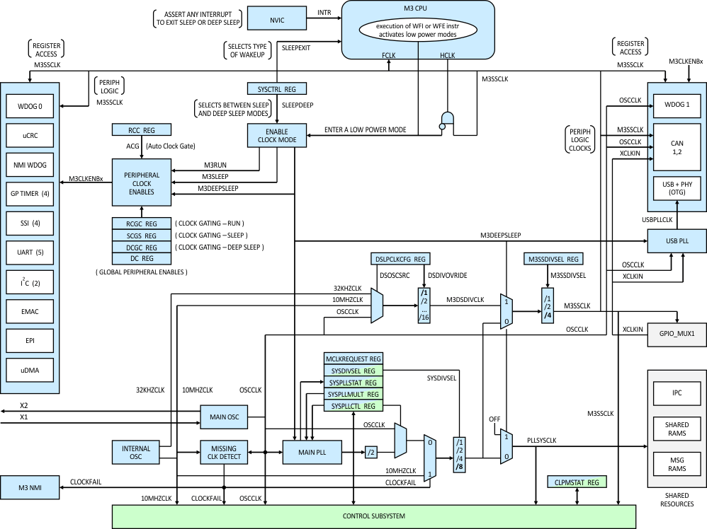
F28M36P63C2 F28M36P53C2 F28M36H53B2 F28M36H33B2 m3_clocks_prs825.gifFigure 6-10 Cortex-M3 Clocks and Low-Power Modes
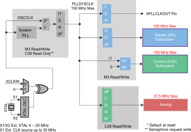
F28M36P63C2 F28M36P53C2 F28M36H53B2 F28M36H33B2 SYSCLK_PLL_prs742.gifFigure 6-11 System Clock/PLL