JAJSVD5C August 2014 – October 2024 FDC1004
PRODUCTION DATA
- 1
- 1 特長
- 2 アプリケーション
- 3 概要
- 4 Pin Configuration and Functions
- 5 Specifications
- 6 Detailed Description
- 7 Applications and Implementation
- 8 Device and Documentation Support
- 9 Revision History
- 10Mechanical, Packaging, and Orderable Information
パッケージ・オプション
メカニカル・データ(パッケージ|ピン)
サーマルパッド・メカニカル・データ
- DSC|10
発注情報
6.5.2 Read/Write Operations
Access a particular register on the FDC1004 by writing the appropriate value to the Pointer Register. The pointer value is the first byte transferred after the target address byte with the R/W bit low. Every write operation to the FDC1004 requires a value for the pointer register. When reading from the FDC1004, the last value stored in the pointer by a write operation is used to determine which register is read by a read operation. To change the pointer register for a read operation, a new value must be written to the pointer. This transaction is accomplished by issuing the target address byte with the R/W bit low, followed by the pointer byte. No additional data is required. The controller can then generate a START condition and send the target address byte with the R/W bit high to initiate the read command. Note that register bytes are sent MSB first, followed by the LSB. A write operation in a read only registers such as MANUFACTURER ID or SERIAL ID returns a NACK after each data byte; read/write operation to unused address returns a NACK after the pointer; a read/write operation with incorrect I2C address returns a NACK after the I2C address.
 Figure 6-4 Write Frame
 Figure 6-5 Read Frame
The I2C interface of the FDC1004 is designed to operate with the standard I2C transactions detailed in the I2C specification; however it is not suitable for use in an I2C system which supports early termination of transactions. A STOP condition or other early termination occurring before the normal end of a transaction (ACK) is not supported and can corrupt that transaction and/or the following transaction.
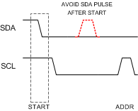
The device is also sensitive to any extraneous pulse on SDA during the SCL low period of the first bit position of the I2C address byte. To ensure proper operation of the FDC1004, make sure the controller device does not transmit this type of waveform. An example of an unsupported I2C waveform is shown in Figure 6-6.
 Figure 6-6 Extraneous Pulse on SDA between I2C START and ADDR